Technology
PCB Technology
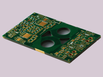
An overview of the PCB Manufacturing can be found here: Heavy copper PCB board, Microvia HDI PCB, High frequency pcb & RF PCB, Metal core PCB and IGBT Ceramic PCB.
Heavy copper PCB Technology
Heavy copper PCB is a circuit board with a copper thickness that is ≥ 3oz per sq. ft in its outer and inner layers. What makes a circuit board classified as a heavy copper PCB is its thicker plating. During the production of heavy copper PCB, copper thickness is enhanced through plated holes and sidewalls. For instance, when a PCB has 2 ounces of copper per sq. ft thickness, it is a standard PCB. However, if it has more than 3oz of copper, it is a heavy copper PCB. Heavy copper PCB is considered a reliable wiring option. Heavy copper PCB is different from extreme copper PCB which features within 20 oz to 200 oz per sq. ft.
Heavy Copper PCBs are widely used in various products as they provide multiple features for improving circuit performance. These PCBs are widely used in high power equipment such as transformers, heat sinking, power inverters, medical equipment, solar panels, automotive products, welding plants, and power distribution systems.

HDI PCB Technology
HDI PCB (high-density interconnection board) is a compact circuit board designed for small capacity users. Compared with ordinary PCB, the most significant feature of HDI is that the wiring density is high.
HDI PCB Manufacturer & Assembly – One-stop service The HDI PCB is defined as a micro via with a hole diameter of 6 mils or less and a hole diameter of 0.25 mm or less. The contact density is above 130 points/square, and the wiring density is with a line width/pitch of 3 mil/3 mil or less. HDI PCB, the full name is High Density Interconnect PCB, it requires much higher wiring density with finer trace and spacing, smaller vias and higher connection pad density. Blind and buried vias’ design is one of their marked feature. HDI PCB board is widely used in Cell phone, tablet computer, digital camera mother board PCB, GPS, Automobile board, LCD module and other different area.
HDI pcb is the abbreviation for High Density Interconnect pcb or High Density pcb. An HDI PCB is defined as a printed circuit board with a higher wiring density per unit area than a conventional PCB. Hitech Circuits Co., Limited is a professional high density interconnect pcbs, HDI pcb board manufacturer, supplier and design company from
High Speed Digital PCB Technology
We Always Perform Signal Integrity Analysis for High Speed PCB
The digital circuit is a powerhouse and high-speed PCBs are full of microprocessors and other components that are managing billions and billions of operations each second. That means any flaw or error in design can cause a significant issue and prevent proper operation.
It’s important for any high speed PCB to be properly engineered to reduce flaws through elements such as impedance discontinuities in transmission lines, improper plating of the through-hole interconnections or other losses of PCB signal integrity.
Hitechpcba has the experts on-hand to achieve the results you need. We know most digital, high-speed applications have long since risen above the operational efficiencies offered by standard FR-4 materials, so we’ll make the right recommendations and prevent you from having performance issues.
High Frequency PCB and RF PCB Technology
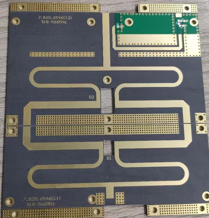
High Frequency PCB and RF PCB with high frequency laminates can be difficult to design because of the sensitivity of the signals, especially compared to other digital signals.
Here are a few things to consider that ensure your design is efficient and minimizes the risk of failures, signal disruptions and other intrusions.
RF and microwave signals are very sensitive to noise — much more sensitive than very high-speed digital signals. That means you’ll need to work to minimize noise, ringing and reflections while treating the whole system with care.
Return signals take the path of least inductance — ground planes underneath your signal will make it easier to guarantee this path.
Impedance matching is important. As the RF and microwave frequencies move higher, tolerance becomes smaller. Often, your PCB driver will need to be fixed, such as at 50 ohms, and that means 50 ohms out from the driver, during transmission and sending to the receiver.
Transmission lines that bend due to routing constraints should use a bend radius that’s at least three-times larger than the center conductor width. This will minimize characteristic impedance.
Return loss must be minimized, whether it’s caused by signal reflection or ringing. A return path will always be found, but your design should guide it and prevent bleeding of the return through the PCB’s many layers.

Metal Core PCB Technology
Metal core PCB is an aluminum-based copper clad laminate with good heat dissipation function. Generally, the single layer aluminum-based PCB is composed of a three-layer structure, which is a circuit layer (copper foil), an insulating layer and a metal base layer. Also used for high-end use is designed as a double sided and multilayer aluminum PCB.
A metal core PCB is a special PCB having a metallic base layer. This base layer is usually made of aluminum or copper. As it contains a metallic layer, it is named Metal Core PCB (MCPCB).
IGBT Ceramic PCB Technology
Ceramic PCBs are better than ordinary PCBs due to their heat dissipation performance, current-carrying capacity, insulativity, coefficient of thermal expansion, etc. so they are widely used in various fields. So what are the application areas of ceramic PCBs?
High-power power electronic module
High-power semiconductor modules are a combination of certain functions and modes. Whether it is an insulated gate bipolar transistor (IGBT) or a DC high-power module, ceramic PCB is one of the main core components and has a very large heat dissipation requirement. No matter how heat is generated, the first contact point of the heat is the substrate, so aluminum nitride ceramic PCB is undoubtedly the best choice.

 Chinese
 English
 Russian
 Spanish
 Portuguese


