 Chinese
 English
 Russian
 Spanish
 Portuguese
HDI PCB Design
Excellent Quality
- 100+ PCB Design & Layout projects per year
- Outstanding designers with 10+ working experiences.
- 7/24 Live sales & tech support
- 6 hours PCB Layout expedite services
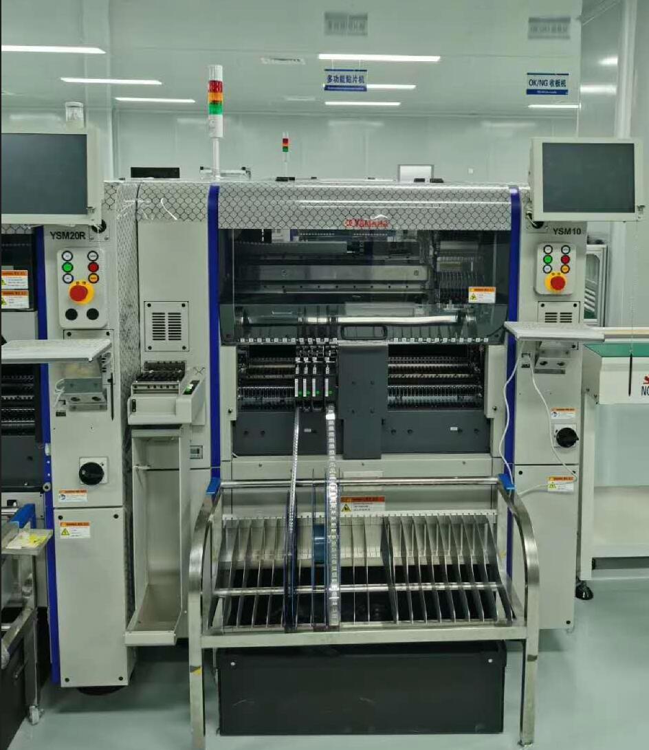
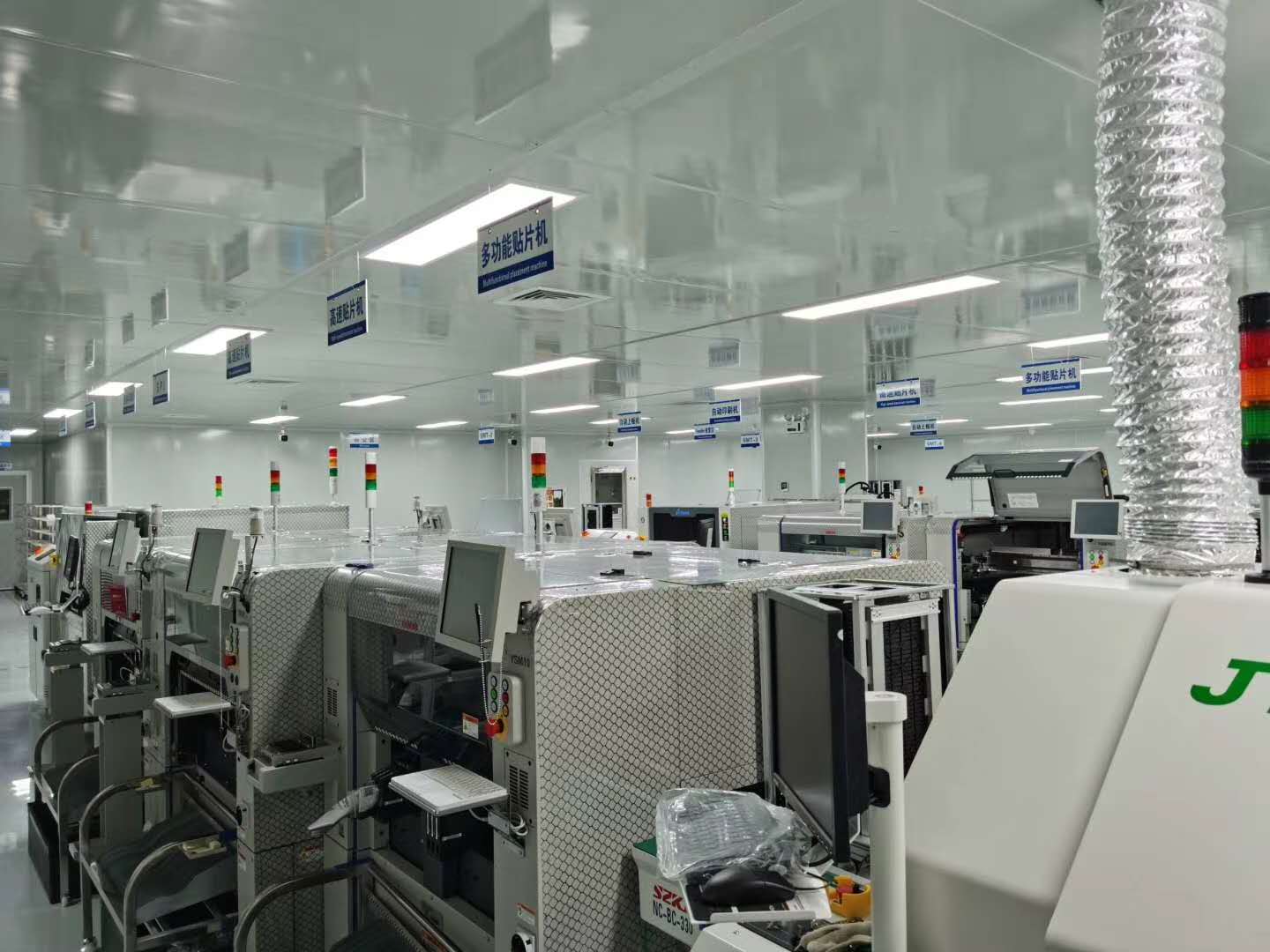
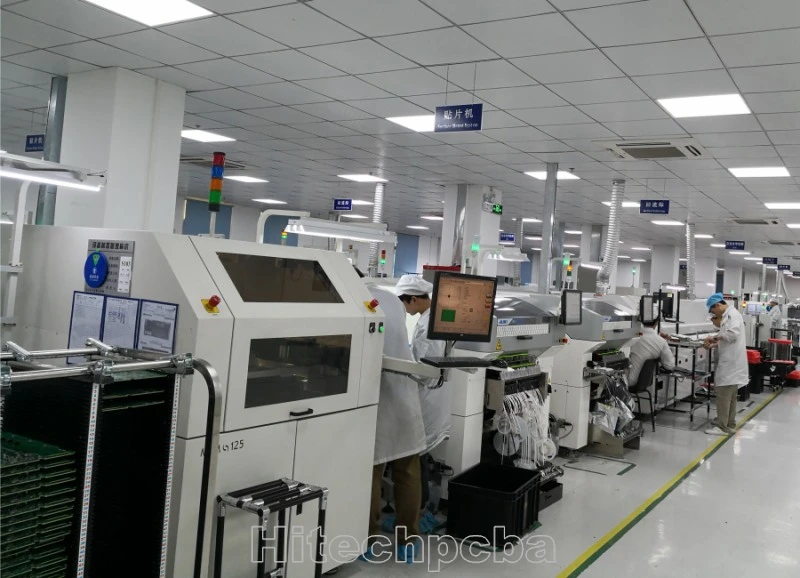
Company Show

Advantages Of Our PCB Design
- Min.trace width 2.5mil,
- Min trace spacing 2.5mil,
- Min vias 6mil ( 4mil laser drilling),
- Max layer count 38 layers,
- Min BGA spacing 0.4mm,
- Max BGA Pin 2500pin,
- HDI highest Layer count 18 layers,
- Fastest delivery time 6 hours per item.
HDI PCB Design
HDI PCB design guidelines
High density interconnect boards, popularly known as HDI PCBs are becoming more popular in the electronics industry. These boards offer high performance and are specially designed for some specific applications. Modern devices are becoming more compact and also the components in these devices are becoming smaller. The invention of the HDI circuit board has contributed to this development.
HDI PCB design and manufacturing began in 1980. Then, researchers needed to investigate how to minimize the via size in printed circuit boards. Since then, manufacturers and designers have looked for ways to populate a single board with more components and functions.

What is HDI PCB?
High density interconnect (HDI) PCB is type of circuit board with higher wiring density for each unit surface area. This density is more than that of a standard board. Also, HDI boards have finer lines and space. They comprise minor vias which can capture pads.
HDI board integrates minimum layers and thin materials for its composition. Therefore, these help to enhance its efficiency and performance. HDI PCB layout is suitable for complex designs. Also, HDI boards offer a lot advantages. These boards enhance electrical performance and reduce the size and weight of equipment.
The vias in HDI PCBs are equal to or less than 150 micrometers. Also, the spaces and lines in these boards are equal to or less than 100 micrometers. All these contribute to the reduced size of HDI boards. Furthermore, the increased interconnection density of HDI PCBs helps to improve signal strength and as well increase reliability. HDI PCBs integrate ultra thin materials and very minimum layers compared to standard PCBs.
HDI PCBs contributed to the development of more powerful and smaller electronic devices. When the lines on a circuit become much smaller than 65 microns, therefore, the possibility to etch your space and trace reduces. For instance, etching on a standard PCB enables a thick resist and there are much spaces for tolerances to etch those spaces.
Definition of HDI circuit boards
In the IPC-6012 it is considered an HDI PCB when the electrical connections on average reach a number of 20 connections per cm2, on both sides of the core and generally to reach these conditions, microvia tracks and gaps should not exceed 100 um. If we think that the parameters described are developed on all layers of the circuit, we understand that it poses great technological challenges for PCB suppliers.
HDI circuit board - technical illustration | Hitech Circuits

Fig 1 Here we show you the current situation that Hitechpcba can support, type III structures based on a central nucleus called NB + 3 sequences of blind holes, NB +4 and +5 sequences will soon be available Including the ELIC structure up to 10L (ELIC = EVERY LAYERS INTERCONNECT)
HDI PCBs are usually classified by the HDI builds, and there are the 1+N+1, 2+N+2, 3+N+3, 4+N+4, and ELIC HDI PCB( Every Layers Interconnect HDI PCB). In the HDI PCB's outer layers, microvias usually form the more expensive stacked vias or cheaper staggered vias.
HDI PCB has a Symmetrical Structure: Inner and Outer Circuit Layers
Each HDI PCB consists of inner and outer layers. Usually, an HDI PCB has a symmetrical structure. The inner layers are the symmetry axis part of the PCB, and usually, this part is penetrated by buried vias. The outer layers clamp the inner layers. They are separately penetrated by blind microvias. For example, in the below simplest 4-layer HDI PCB structure, the upper and bottom layers are the HDI PCB's outer layers, and layers 2 and 3 are the inner layers.

HDI PCB Builds: 1+N+1, 2+N+2, 3+N+3, 4+N+4, 5+N+5 and ELIC HDI PCB
HDI builds means how many times of laser drilling for microvias. 1+N+1 is the simplest HDI build, and it means the HDI PCB's microvias are single vias that need only one laser drilling.
2+N+2 means the HDI PCB needs twice laser drilling, and both the upper and bottom outer layers have 2 PCB layers. Unlike 1+N+1, 2+N+2 has two cases. One is that the microvias of the two adjacent outer layers overlap, and the two microvia form a stacked via. The other case is that the microvias of the two adjacent outer layers do not overlap, and they form a staggered via. As we know, it requires extremely high precision to locate and pile up two microvias, so stacked via HDI PCBs are more expensive than staggered via HID PCBs.

3+N+3 means the HDI PCBs need three times of laser drilling and both the upper and bottom outer layers have 3 PCB layers. And so on. The more times of laser drilling, the higher requirements for HDI PCB manufacturing technologies and more costs. 1+N+1, 2+N+2, 3+N+3, and 4+N+4 HDI PCBs are used commonly. 5+N+5 HDI PCBs are also in use but less. For example, iPhone 6 uses the 5+N+5 HDI PCB as its mainboard.
ELIC HDI PCB means Every Layers Interconnect PCB
Are you designing high-density interconnect PCBs?
HDI PCBs are characterized by their high density of components and routing interconnections, using the latest design and manufacturing technologies.
An HDI PCB is a high-performance board that takes advantage of
Laser microvias
Blind and buried vias
Fine lines and spaces
Via-in-pad technology
Built-up and sequential PCB laminations
Fine pitch devices down to 200 microns
And HDI PCB design is a critical process that necessitates expertise, experience, and the proper utilization of technology. In order to aid in your understanding of HDI layout and facilitate successful HDI PCB design, we are sharing some key considerations and suggestions to keep in mind during the design process in this blog, with the hope of inspiring you to create innovative HDI designs.
What Is HDI Layout?

HDI PCB design is a specialized approach that optimizes component placement on a printed circuit board (PCB) to maximize space utilization and minimize signal interference. It is particularly beneficial for designing compact and high-performance electronic devices like smartphones, tablets, and wearables.
There are various types of HDI layouts, including the sequential build-up, stacked vias, and microvias. In the sequential build-up, layers of the PCB are built up sequentially to achieve the desired density. Stacked vias involve drilling holes through multiple layers of the board to create interconnections. On the other hand, microvias are similar to stacked vias, but they are much smaller in size, allowing for even higher component density on the PCB.
Why is HDI PCB Important in Electronic Manufacturing?
There are various benefits of HDI technology. First of all HDI technology helps to reduce the size of devices due to the high connection pad density. Also, HDI PCBs enhance performances of devices. HDI technology contributes to the manufacturing of wearable electronics, handheld electronic devices, and smartphones. Furthermore, the ability to integrate more components in electronics makes HDI PCBs are preferred option among manufacturers.
Smaller weight and size
HDI PCBs enable the production of smaller devices. This is because these boards allow the integration of more components. With reduced board size, manufacturers can build devices that can fit into smaller spaces.
Enhanced signal transmission
High density PCB enhances signal transmission. Also, these boards improve signal quality in electronic devices.
Denser trace routing
HDI PCBs enable manufacturers to integrate more components on the circuit board. This enables denser trace routing. Also, HDI PCB design offers more freedom to freedom to integrate more components on both sides of the board.
High reliability
HDI PCBs are very reliable as a result of its integration of stacked vias. Also, HDI boards offer great protection against any extreme environmental conditions.
Cost effective
HDI technology offers cost effective solutions for electronics production. Quality is a crucial factor when designing electronics. HDI design makes it possible to minimize a standard 8 layer PCB to a 4 layer HDI PCB through the use of microvia. Also, a well-designed 4 layer HDI PCB can offer better functions more than an 8 layer standard PCB.
HDI PCB Design Considerations
Use of microvias
The use of microvias can help PCB designers to achieve more number of pins. Also, microvias can create the escape area of dense components. Microvias feature low inductance which makes them ideal for high-speed applications. Also, they help to link power planes with decoupling capacitors.
Component selection
An HDI PCB usually comprises SMD and BGA components. Also, it is crucial to choose the pitch/spacing between these pins. Proper spacing between pins helps to define board stack-up and trace widths.
Material selection
This is an important consideration for every PCB design. However, it is a more crucial consideration in HDI PCB design. Selecting the appropriate material is ideal for manufacturability and also meeting electrical requirements.
Thermal management
The IPC-2226 standard points out thermal issues in circuit board. Therefore, it is advisable to refer to this standard to ensure better thermal management. Also, designer needs to prevent these thermal issues. Thinner dielectrics can ensure thermal dissipation. It is advisable you add thermal vias to increase dissipation.
Testing
Rather than using In-circuit testing, HDI PCB designers integrate JTAG or functional testing. This is because in-circuit testing usually requires full nodal analysis.
Vias capping
It is advisable you cap or fill microvias to offer a planar surface. Also, capping of vias enables designers to place active parts on the two sides of the PCB. Failure to cap your vias can cause air bubbles and this will affect the quality of solder joint.
Minimized plane perforation
Bigger ground or power copper are enhances power integrity and electromagnetic compatibility. However, microvias create a small gap wherever they perforate a plane and this can have effects on power integrity, signal integrity, and electromagnetic compatibility. Therefore, perforate less to get higher shielding and better image plane effect.
The Trends and Future of HDI PCB Technology
In life, humans will always demand for changes. Change is a constant thing in life. Constant change, innovation, and development keep happening in the electronics industry. The advent of HDI PCB technology has led to development in electronics manufacturing. Almost all industries benefit from HDI printed circuit board technology.
In the past, printed circuit boards comprise several conductive layers. Things have changed as this is no longer the case. For HDI board technology, the future seems bright. More complex and compact devices will be manufactured. The capability of HDI boards to integrate more components on both sides will make this possible.
Furthermore, blind via and via-in-pad technologies will aid this development. Devices that will be primarily manufactured with HDI circuit boards will transfer signals faster and reduce signal loss. Also, the integration of laser drilling in HDI circuit boards enhances their capabilities. HDI printed circuit boards have fine pitch components.
HDI printed circuit boards minimize the number of conductive layers for a circuit board, thereby reducing dense trace routing. Also, HDI PCBs integrate microvias, buried, and blind vias which enhances routing within a small space. Due to this capability, there is minimized distributing inductance. Hence, this enhances signal integrity.
Also, the HDI PCB technology enabled alternative stack up techniques due to the integration of buried vias, blind vias, and microvias. The integration of drilled sequential lamination has helped manufacturers to increase the density of boards.
HDI has several technological impacts in the PCB industry. One of such is the reduction of the number of layers and size of a board. Therefore, this enhances conductivity.

Crucial Things to Understand in HDI PCB
Microvia Hole
A microvia hole is a blind hole created on the conductor-insulator multilayer. It creates electrical connection via an insulator in the conductive layers.
Minimum pad size hole
The minimum pad size hole on the internal or external layer of an HDI PCB should be +0.010. However, the pad size hole should be +0.014 for the component holes.
Copper wrap
Copper wrap refers to the copper layer that shields the filled holes’ outer surface. Also, the copper wrap’s thickness depends on the outer surface copper thickness of the plated hole.
Recommended via hole plugging
The hole plugging resin always fill the via holes. A permanent hole filling substance will fill this hole.
Capped via hole
The surface’s flatness determines the via in pad design. Also, the holes will be filled with resin. Therefore, you will need an additional thin copper cap.
Use Cases of HDI PCB
HDI PCBs have several use cases. They are popularly used in high performance applications since they offer dense circuitry. Also, they are highly preferred in most industries since they minimize the size of devices.
Consumer electronics
The complex and compact consumer electronic devices you see today feature HDI PCB. Also, high density interconnect (HDI) technology has contributed to the development of digital smart phones. These boards have contributed to the advancement in laptops and personal computers. Other electronic devices like LED TVs, touch screen devices, and digital cameras have benefited from HDI printed circuit board.
Aerospace
Most devices in the aerospace industry feature HDI PCBs. Effective heat dissipation in aerospace devices is crucial. Hence, this calls for a higher density interconnect board. HDI circuit board is widely integrated for manufacturing communication and navigation devices in aerospace devices.
Medical
A wide range of medical devices feature HDI printed circuit board. For instance, medical equipment like scanners, colonoscopy camera, and heart monitors comprise HDI boards. Colonoscopy cameras go through the colon of human for examination.
Automotive
The automotive industry is one of the industries that rely on HDI boards. Vehicle manufacturers are highly interested in these boards due to the fact that it enables more innovations. With HDI circuit board, you can save space and as well enhance the performance of a vehicle. Also, vehicles like Tesla integrated HDI PCBs to manage electric functions.
Conclusion
In conclusion, HDI PCB design is a critical process that requires careful consideration of various factors. By following the HDI PCB design guidelines and considering the key factors mentioned in this blog, designers can create innovative and reliable HDI designs and enable the realization of innovative and cutting-edge products.
HDI PCB design requires the consideration of some factors. Revolutionary new devices like wearables, small footprint gadgets, and touch screen computers all integrate HDI PCBs. High density interconnect boards are gradually becoming the mainstay of the electronics industry.
Hitech Circuits, a leading PCB manufacturer in

0086-755-29970700
sales@hitechpcb.com; sales@hitechcircuits.com
2F, Building C, Suojia Technology Park, Hangcheng, Bao’an, Shenzhen, Guangdong, China 518126


