 Chinese
 English
 Russian
 Spanish
 Portuguese
Rigid-Flex PCB Design
Excellent Quality
- 100+ PCB Design & Layout projects per year
- Outstanding designers with 10+ working experiences.
- 7/24 Live sales & tech support
- 6 hours PCB Layout expedite services
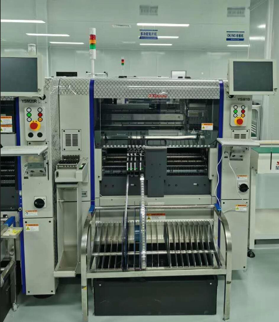
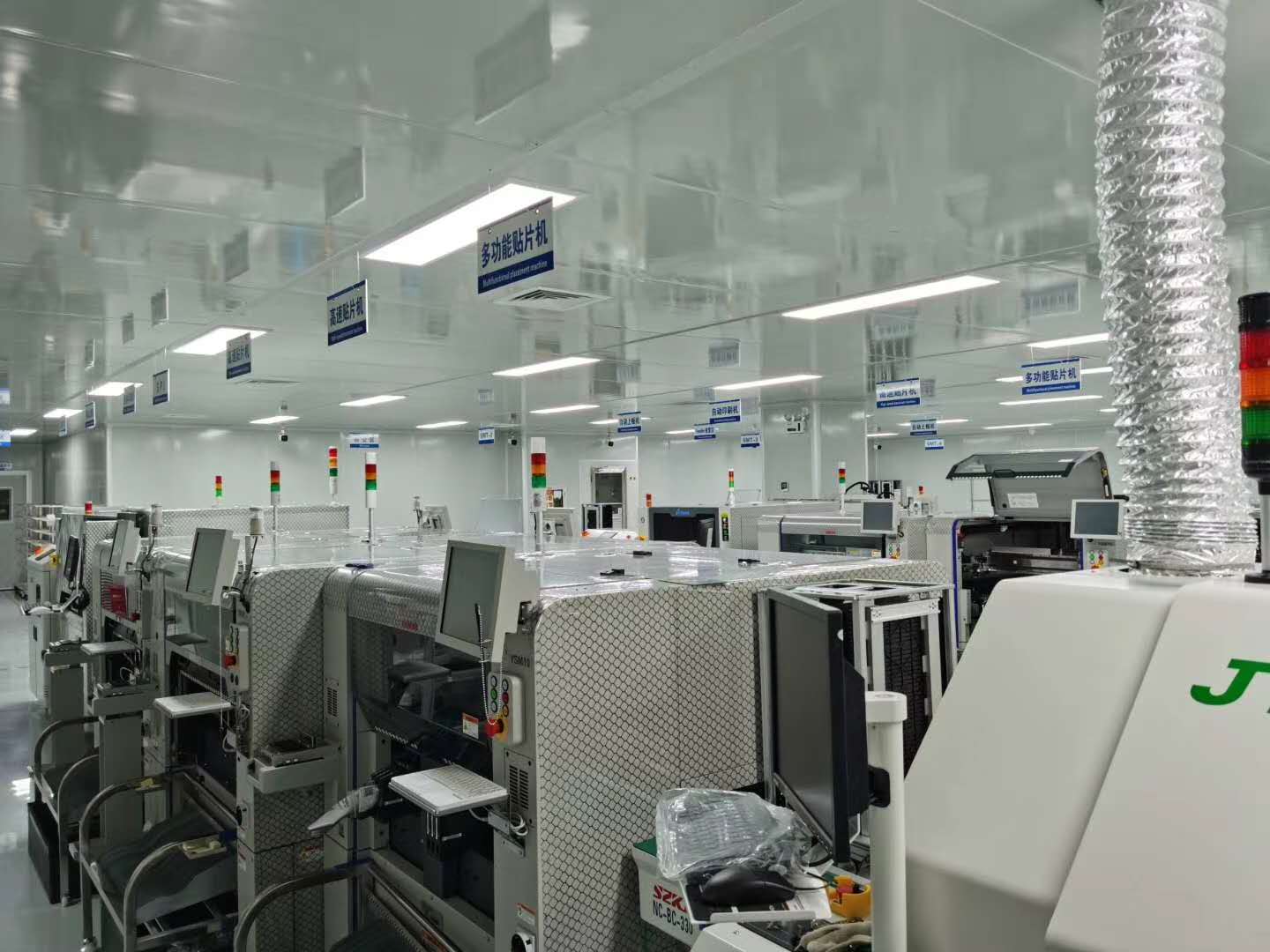
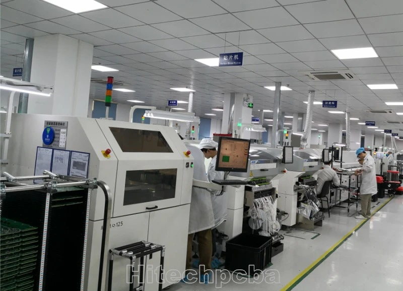
Company Show

Advantages Of Our PCB Design
- Min.trace width 2.5mil,
- Min trace spacing 2.5mil,
- Min vias 6mil ( 4mil laser drilling),
- Max layer count 38 layers,
- Min BGA spacing 0.4mm,
- Max BGA Pin 2500pin,
- HDI highest Layer count 18 layers,
- Fastest delivery time 6 hours per item.

Rigid-Flex PCB Design
Rigid flex PCB design guidelines
What is Rigid Flex Boards?
Rigid flex boards are a combination of both flexible and rigid circuit boards. Also, typical methods to manufacture them are similar to those utilized on circuits of rigid boards.
However, some of these layers feature a flexing or flexible circuitry that runs from this rigid board into the board. Then the manufacturer makes use of a plated hole in the boards linking the layer of the rigid circuit to the region of the flexible circuit.
This configuration leads to a rigid flex pcb, which you can install easily as a rigid board. Also, for products having limited room, it can be folded easily. Furthermore, the devices have a flex-ability feature that can be referred to in some cases as dynamic flexion.

Rigid Flex PCB Manufacturer
To reassure the ultimate reliability as a leading Rigid Flex PCB manufacturing company, our rigid-flex PCBs are specially designed for the rigors of aerospace, medical applications. Flex assemblies also reduce connectors, and the manufacturing labor, yield, transmission, and reliability issues that are inherent as part of their application. Please link here to learn more about rigid flex pcb design guidelines.
Quick turn rigid flex PCB board manufacturing within 10 working days.
The fastest Turn-Key Rigid Flex PCB assembly within 2 weeks.
Stacked and staggered Micro via large format circuit board
Large format Circuit board
Ultra long rigid flexible PCB board
Heavy copper Rigid Flex PCB Copper Weight of up to 10 oz
Sculptured rigid flex circuits
Copper-filled microvias Rigid Flex PCB
Minimum track width and spacing in mass production around 50μm
HDI Rigid Flex PCB build up: 1+N+1 HDI Rigid Flex PCB, 2+N+2 HDI Rigid Flex PCB, 3+N+3 HDI Rigid Flex PCB, 4+N+4 HDI Rigid Flex PCB
Any layer HDI Rigid Flex PCB
Ultra-thin HDI Rigid Flex PCB for wearable electronics
Material Layout Considerations for Rigid Flex PCB Design
Before you begin a design, it is advisable to reach out to your manufacturer. Depending on if the printed circuit board is for stable bend or dynamic bend, there may be differences in the choice of bend radius, layers, coverlays, and copper type.
Rigid flex PCBs of dynamic bend are usually installed in environments where you can subject it to bending constantly. Therefore, a great recommendation will be to use a maximum of 2 layers. Also, make sure that the radius of the bending is at about 100 times the thickness of the material.
For example, having about 10 – 20 layers of rigid flex PCB that should serve stable-bond installations is possible. It will not be made to undergo continuous bending force. This means having a bending radius of 10 times the material thickness is possible as well.
Furthermore, the flexible material’s flex lay up has a huge effect on the costs to manufacture them as well as the PCB’s final performance. Therefore, it is important to choose the best material possible. Moreover, some major considerations in both the choice of material and copper weights include controls on load-carrying requirements and impedance resistances.
Also, there is a need to collaborate with the assembler to discuss the design of your PCB. This is to make sure that all the components work in line with the requirements of signal integrity.

Rigid Flex PCB Design Guidelines
Rigid flex designs closely resemble the rigid board design. Also, its flexible layers usually extend fully into the board’s rigid layers. Like rigid board layouts, the fabrication package of the rigid flex will include solder mask layers, cover layer, drill files, gerber layers, perimeter files, nomenclature, etc.
However, the fact is that some major differences exist between the rigid flex’s PCB’s fabrication packages as well as the rigid board applications.
Generally, rigid flex PCBs feature more dimensions. Therefore they should define their requirements carefully, because these boards are useful in 3D applications. Also, it should define the rigid to the flex transition areas accurately. This is because they are not usually apparent when you are viewing these Gerber layers only.
Also, the rigid flex board’s material layup is critical. Therefore, you have to team up with the fabricator to work it out. Your fabrications will help you choose the right materials. This will be based on your requirements like mechanical considerations, RoHS certification, impedance control on the rigid and flex layers, minimum bend radius necessary, compatibility of the lead free assembly process, as well as other considerations.
Usually, the rigid flex boards assembly needs the Gerber files to have additional layers. The layers will feature the solder mask layers. However, if the board requires it, there’s also a need for the artworks layers, which define the bondply and coverlayer sections.
Other Guidelines
Bending areas shouldn’t have plated through holes
Also, the bending areas shouldn’t have plated through holes. Areas around the bending lines usually deliver a form of mechanical stress, which could affect its structure. You can run or place vias and pads on areas which are not made to undergo bending, though not recommended. In cases like this, strengthen your plated holes using anchors. In addition, use teardrops in connecting the trace and the plated hole. This ensures stronger joints. Also, this practice of using larger vias and pads is a good one.
Make use of Cross-hatched ground plane
Deciding to pour ground planes as copper’s solid area, then you are risking placing huge stress on it. This can also reduce its flexibility. Rather, on the PCB’s flex area, making use of a cross-hatched ground plane is suitable. Also, make use of reliable software for your PCB design, which backs the designed guidelines of the rigid flex PCB. This helps you create a prototype that is error-free.
Conclusion
We hope we have been able to give you ideas of what flex pcb board design is and its significance in rigid flex pcbs. Make sure that you work with the material considerations and take note of all you need to know before embarking on a PCB design. Also, we have added some guidelines to help you throughout the design process. This will increase the PCB’s capabilities. To have a full understanding of this topic, you can read it over again. You can visit our blog for other related topics.

0086-755-29970700
sales@hitechpcb.com; sales@hitechcircuits.com
2F, Building C, Suojia Technology Park, Hangcheng, Bao’an, Shenzhen, Guangdong, China 518126


