 Chinese
 English
 Russian
 Spanish
 Portuguese
Heavy Copper PCB Design
Excellent Quality
- 100+ PCB Design & Layout projects per year
- Outstanding designers with 10+ working experiences.
- 7/24 Live sales & tech support
- 6 hours PCB Layout expedite services
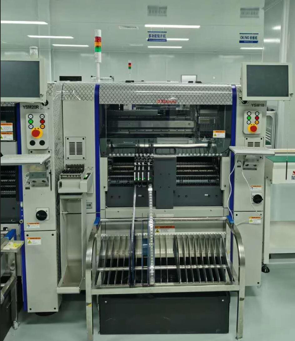
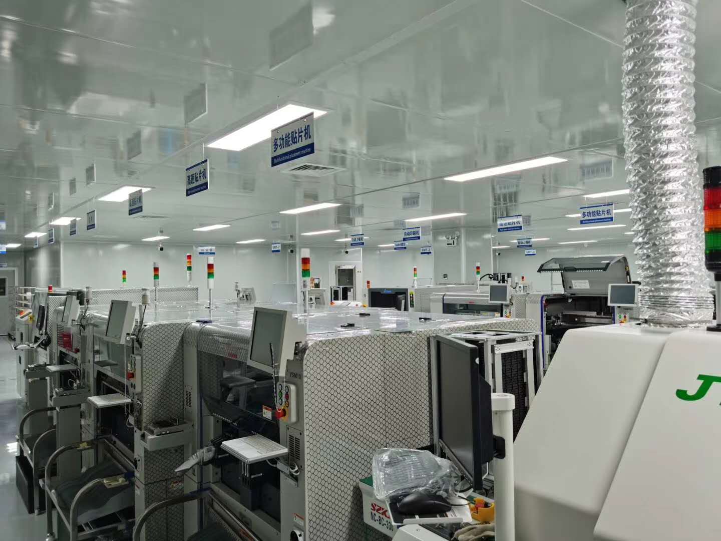
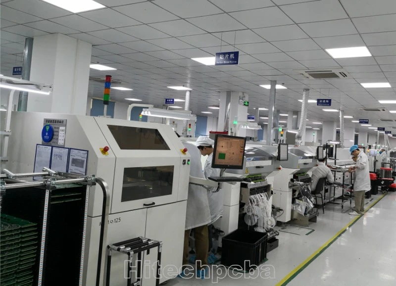
Company Show

Advantages Of Our PCB Design
- Min.trace width 2.5mil,
- Min trace spacing 2.5mil,
- Min vias 6mil ( 4mil laser drilling),
- Max layer count 38 layers,
- Min BGA spacing 0.4mm,
- Max BGA Pin 2500pin,
- HDI highest Layer count 18 layers,
- Fastest delivery time 6 hours per item.

Heavy Copper PCB Design
Heavy Copper PCB Design
Current industrial requirements are increasingly requiring heavy copper PCB design. These PCBs have found growing usage in the electronics sector, notably in complex switches that must fit into a compact area. This is owing to copper’s strong electrical and thermal conductivity. The end product is a multi-layered or double-sided board with detailed exterior layer(s) and heavy copper layers on the interior layers. As a result, these boards may be found in both power converters and planar transformers.
Heavy Copper PCB Overview
A heavy copper PCB is a board that has a heavy copper circuit. This kind of PCB is subjected to specialized plating and etching techniques such as step plating and differential etching. It is also referred to as a thick copper PCB. After all, copper weights range from 4 oz/ft2 to 20 oz/ft2.
As a result, there is no need to create high-current/high-power circuits and control circuits on separate boards with the thick copper board. In addition, the thick copper plating comes with a simple board design and is highly dense.

Heavy Copper PCB Design Steps
When designing Heavy Copper PCBs, there are several key factors to keep in mind. Here are some tips and tricks to consider:
Determine your requirements: Before you start designing your Heavy Copper PCB, you need to determine the specific requirements of your application. This includes the amount of current the PCB needs to carry, the operating temperature, the size and shape of the PCB, and any other unique requirements.
Choose your materials: Heavy Copper PCBs require specialized materials, including high-quality copper foils and laminates. You should also consider the thickness of the copper layers and the substrate material used for the PCB.
Plan your layer stack-up: The layer stack-up is an essential part of the Heavy Copper PCB design. You should carefully plan the layer stack-up to ensure proper heat dissipation and signal integrity. Consider the placement of copper layers, dielectric layers, and any other necessary layers.
Determine trace width and spacing: Heavy Copper PCBs require wider copper traces to handle the high currents. You should also increase the spacing between traces to avoid electrical arcing. Consider the specific requirements of your application to determine the appropriate trace width and spacing.
Consider thermal management: Heavy Copper PCBs generate a lot of heat, so you need to consider how to dissipate that heat efficiently. This can include using thermal vias to transfer heat from the copper layers to the outer layers of the PCB, or using specialized thermal management techniques such as heat sinks or fans.
Ensure manufacturability: Heavy Copper PCBs require specialized manufacturing processes, so it’s essential to ensure your design is manufacturable. This includes ensuring the drill holes are in the right locations and of the correct size, the plating is of high quality, and the overall design meets the manufacturer’s specifications.
Heavy Copper PCB Design Tips
When it comes to designing Heavy Copper PCBs, there are several important considerations to keep in mind. Here are some tips and tricks that can help you design a high-quality Heavy Copper PCB:
Layer stack-up: Heavy Copper PCBs require careful layer stack-up design to ensure proper heat dissipation and signal integrity. You want to place the copper layers as close as possible to the center of the PCB to reduce thermal resistance and maximize heat transfer.
Trace width and spacing: Since Heavy Copper PCBs are designed to handle high currents, you need to ensure that the copper traces are wide enough to carry the current without overheating. You should also increase the spacing between the traces to avoid electrical arcing.
Drilling and plating: Heavy Copper PCBs require specialized drilling and plating processes to ensure a reliable connection between the copper layers. You should use high-quality plating materials and select the right drill bit size to ensure precise drilling.
Thermal management: Heavy Copper PCBs generate a lot of heat, so you need to consider how to dissipate that heat efficiently. You can use thermal vias to transfer heat from the copper layers to the outer layers of the PCB, or you can use specialized thermal management techniques such as heat sinks or fans.
Quality control: Heavy Copper PCBs require strict quality control measures to ensure they meet the performance and reliability requirements. You should conduct extensive testing and inspection throughout the manufacturing process to detect any defects or issues.
By following these design tips and tricks, you can create a high-quality Heavy Copper PCB that meets the performance and reliability requirements of your application.

What Does Heavy Copper PCB Offer?
Why should you use a heavy copper PCB? Here are a few of the advantages:
Multi-use:
Not every board can endure the weight of the heavy copper PCB without sacrificing board quality or performance. These boards are more likely to be utilized across various devices with variable power and signal levels than regular PCB boards.
Compact size:
Heavy copper boards’ capacity to sustain frequency, high current, high temperature, and recurrent thermal cycles is attributable to many layers’ stocking attributable to many layers’ stacking onto a single layer. This decreases the board’s total size and weight, enabling tiny, high-performance circuits to be used.
Resistant to thermal degradation:
High-frequency boards create a lot of heat, which the fan cooling system cannot effectively disperse. This heat damages the board’s fragile soldered joints, lowering performance and finally destroying it. Due to their increased conductivity, heavy copper PCB boards will create less heat and be away from any external heat at a much faster pace.
Improve Load Sharing:
Instead of generating multiple duplicate and parallel layers, heavy copper can be combined with copper vias. This lowers the load-sharing difficulties associated with numerous parallel levels.
The board’s structural advantage:
A multi-layered heavy copper PCB provides increased mechanical strength because of the stacking of layers and the plated-through holes.
How is Heavy Copper PCB Fabricated?
Plating or etching is commonly utilized in the production of extreme copper PCBs. The primary goal is to increase the copper thickness of sidewalls and plated holes. However, normal etching processes result in unevenly etched margins and edge lines. Therefore, specific etching and plating processes are required to achieve the additional thickness of copper on heavy copper PCBs.
Heavy copper PCBs are electroplated throughout the PCB manufacturing process. This will assist in thickening the PTH barriers on the PCB. As a result, the layer count is reduced, and the impedance distribution is narrowed with this method. However, when PCBs are driven to several cycles throughout the manufacturing process, the plated holes might become fragile.
Methods for Fabricating Heavy Copper PCBs
Blue Bar Method: The Blue Bar Method is used to create automobile PCBs. It entails inserting thick copper bars onto PCBs to transmit the additional current. Because just a few lines are needed to carry more significant current in high-power circuits. This approach saves both time and money by reducing the weight of the PCB. On the other hand, fabricators of multi-layer PCBs must pay close attention to the copper fill level between inner layers in order to prevent additional delamination.
Embedded Copper Method: Using this approach, a thick copper PCB with a heavy copper and flat surface incorporated within the prepreg resin is created. The resin thickness determines the thickness of the heavy copper that must be used.
Difference between a Thick Copper PCB and Standard PCB
The thickness of the copper deposition on the board is the significant difference between regular PCB and thick copper PCB.
The copper layer on a standard PCB weighs one ounce or 35 micrometers, but the copper layer on a thick copper PCB weighs four ounces or 140 micrometers.
Standard PCB cannot conduct large current values; however, extreme copper PCB can perform significant current levels.
Furthermore, standard PCBs do not sustain mechanical stress to enhance heat conductivity.
On the other hand, thick copper PCBs are recognized for enhancing heat conductivity while preserving mechanical stress.
Heavy Copper PCB Capabilities
When employing heavy copper PCB for various applications, it’s vital to evaluate its capabilities. Based on its specifications, this sort of PCB is more expensive to build.
Below mentioned capabilities should be available on a heavy copper PCB:
A maximum board size of 457mm x 610mm and a minimum board size of 6mm x 6mm is required.
Copper thickness per square foot is more than 3oz.
Green, black, blue, red, white, purple, or yellow solder masks are recommended.
The color of the silkscreen is either white, yellow, or black.
A board with a thickness of 0.6mm to 6mm
The maximum copper weight for the exterior layer should be 15 ounces.
Immersion Gold, HASL, and OSP should be used for surface finishing.
The final thickness ranges from 0.020 to 0.275 inches.
Applications of Heavy Copper PCB
Heavy copper is widely used in printed circuit boards with high energy (or high current), such as power electronic devices and power supply systems. These PCBs are most observed in the following industries:
Advantages of Heavy Copper PCB:
1- Enhanced survival against high temperatures and thermal strains
2- Improvement in current carrying capacity
3- High mechanical strength
4- Overall size of product is reduced by incorporating high and low power electronics on same PCB.
5- Efficient heat transfer and dissipation
6- Heat-sinks directly plated on the surface of board with up to 120-oz copper.
7- High-power-density planar transformers are printed on board
Heavy Copper PCB Applications:
1- New energy Auto.
2- Lighting Applications example high brightness LED lights, bulbs
3- Industrial Equipment like power supplies, Solar energy, Motor driver circuits, Inverter, UPS, Stabilizers, Battery Chargers, servo drives etc
Choosing the Right Heavy Copper PCB Manufacturers
Design Guide for heavy copper PCB
This article is for design guide about heavy copper PCB (heavy copper printed circuit board) and DFM (design for manufacturing) is the line width and line space for heavy copper PCB (heavy copper printed circuit board), meanwhile the DFM (design for manufacturing) is very important for heavy copper PCB (heavy copper printed circuit board) because most of PCB design guides will not meet heavy copper PCB (heavy copper printed circuit board). Many of PCB suppliers can manufacture PCB with 4 mil ~ 5mil line width and line space as min trace/space, but it is not meet the requests of heavy copper PCB (heavy copper printed circuit board), 3~ 4 mil circuit line width is always for 0.5 OZ or 1 OZ copper layer on PCB, but not for heavy copper PCB (heavy copper printed circuit board) (3 OZ ~ 30 OZ copper PCB), you know PCB manufacturer can’t do 3 mil line space for 30 OZ PCB, this is why PCB designer have to consider the DFM.
Meanwhile, you can visit heavy copper PCB (heavy copper printed circuit board) and FAQ of heavy copper PCB (heavy copper printed circuit board) for more information.
A) Line Space & Line Width on heavy copper PCB (heavy copper printed circuit board)
When design the board, you should consider relationship between Minimum line space (refers to Min LS later) and Minimum line width (refers to Min LW later). And to have a bigger value will make the board easier to be made.

B) Min Plated Through Hole (PTH) Diameter
PTH should be >=0.3mm; copper ring annular: 0.15mm
C) Wall copper thickness for PTH: Normal: 20um-25um, and Max 2-5OZ (50-100um).
D) Max layers: For heavy copper, max layers we can make is 20L.
Board thickness should be >1.6mm for 30OZ copper.
Impedance control, high Tg, are not workable for heavy copper.
Min Via: 0.3mm.
E) Max board size: 550x350mm is the most economical. Bigger size (550x500mm) also workable but cost will be much higher.
If you would like to know more information about heavy copper PCB (heavy copper printed circuit board) or know the questions for heavy copper PCB (heavy copper printed circuit board) in order to avoid mistakes when you design heavy copper PCB (heavy copper printed circuit board),you can visit other pages on our website or contact us for help directly.

0086-755-29970700
sales@hitechpcb.com; sales@hitechcircuits.com
2F, Building C, Suojia Technology Park, Hangcheng, Bao’an, Shenzhen, Guangdong, China 518126


