 Chinese
 English
 Russian
 Spanish
 Portuguese
PCB Stackup
Excellent Quality
- 100+ PCB Design & Layout projects per year
- Outstanding designers with 10+ working experiences.
- 7/24 Live sales & tech support
- 6 hours PCB Layout expedite services
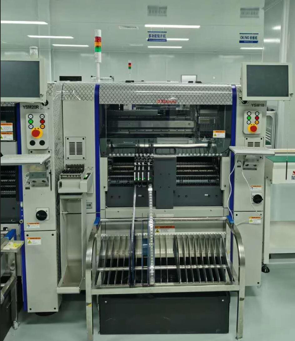
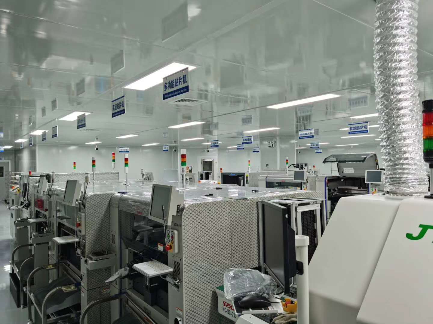
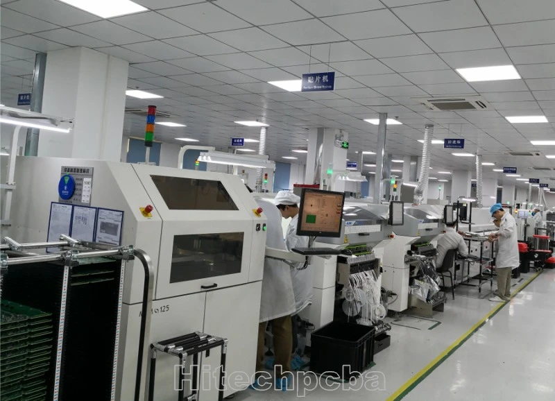
Company Show

Advantages Of Our PCB Design
- Min.trace width 2.5mil,
- Min trace spacing 2.5mil,
- Min vias 6mil ( 4mil laser drilling),
- Max layer count 38 layers,
- Min BGA spacing 0.4mm,
- Max BGA Pin 2500pin,
- HDI highest Layer count 18 layers,
- Fastest delivery time 6 hours per item.

PCB Stackup
What Is PCB Stackup?
PCB stackup refers to the arrangement of copper and insulating layers that constitute a printed circuit board. A typical PCB stackup consists of alternating layers of copper and insulating material, such as prepreg and core layers. The copper layers contain the circuitry and serve as the conductive pathways for the electronic signals on the board.
The PCB stackup is an essential aspect of the board’s design and determines the electrical properties of the board, including signal integrity, power distribution, and electromagnetic compatibility (EMC). It also impacts the mechanical and thermal properties of the board. The number of layers used in a PCB stackup can be flexible and is determined by the complexity of the circuit and the specific design prerequisites.
A two-layer PCB stackup is the simplest and most common, but high-density designs may require four or more layers to accommodate the necessary components and routing. Designers must carefully consider the PCB stackup during the design process to ensure that the board meets the necessary electrical and mechanical requirements while also being cost-effective to manufacture. Proper stackup design can help minimize signal loss, reduce electromagnetic interference, and provide a stable power distribution network, resulting in a more reliable and high-performance circuit board.

A stack up is the course of action of layers of copper and protectors that make up a PCB prior to planning the last design of the board. Dealing with a decent stack up isn’t by and large simple and organizations that make multi-facet printed circuits, for example, Hitech Circuits, a China company committed to the quick prototyping of SMT printed circuits and cross-area segments, for experts, should be at the bleeding edge.
Having numerous layers builds the board’s capacity to convey energy, decreases cross-impedance, wipes out electromagnetic obstruction and supports rapid signs. While a stack up level permits you to get numerous electronic circuits on a solitary board through the different layers of PCB board, the construction of the PCB stack up configuration gives numerous different benefits:
A heap of rigid pcb layers can help limit the circuit weakness to outer commotion, just as limit radiation and abatement impedance and crosstalk issues on fast frameworks
Great PCB stacking can likewise add to effective and minimal expense last creation
A right heap of 4 layer PCB stackup layers can improve the electromagnetic similarity of the task.
With a solitary layer or twofold layer PCB the board thickness is once in a while thought of. Notwithstanding, with the approach of multi-facet PCBs, the heap of materials is beginning to turn out to be increasingly basic and the last expense is the factor that influences the whole undertaking.
The most straightforward stack up can incorporate 4-layer PCBs, up to the more unpredictable ones that require proficient successive overlay. The higher the quantity of layers, the more the architect is allowed to unwind his circuit, with less shot at coincidentally finding “unimaginable” arrangements.
The 4 layer pcb stack up covering tasks comprise in the plan of the copper layers and the protecting layers that make up a circuit. The stack up you pick positively assumes a significant part in the presentation of the board severally.
What are the Advantages of Using the Layer Stackup Design?
Having more than one layer on the printed circuit board will increase the ability of the board to increase energy flow.
Apart from that, the printed circuit board will prevent any form of cross-interference during the application stage.
In addition to that, you will have a printed circuit board that does not experience electromagnetic interferences.
With most of the interferences out of the way, you will have a printed circuit board that performs at high speeds.
This is because of the fact that you will have multiple electronic circuits on the PCB by increasing number of layers.
On top of the above benefits, here are other benefits that you will experience with the layer stackups.
Minimize Circuit Vulnerability
With the layer stackup, you will minimize circuit vulnerability to noise that comes from external sources.
Apart from that, it will minimize cases of radiation while decreasing crosstalk and impedance problems under high-speed applications.
Low-Cost Production
Having a good printed circuit board layer stackup will also help in eliminating the high cost of making PCBs.
It will place multiple circuits on one board thus streamlining production, reducing waste and the overall cost of production.
Improve Electromagnetic Compatibility
You will also be in a better position to operate machines that have great electromagnetic compatibility.
There will be very minimal interferences thus increasing the efficiency of operating the layer stack ups.
What are the Most Significant Factors to Consider When Dealing with Board Stackup?
You need to be very careful especially when you are making or dealing with the board stackup.
This is an important factor that should help in preventing mistakes that increase circuit noise and radiation.
To avoid making such mistakes, you have to consider particular factors when dealing with the stackup of the boards.
Here are the main factors to consider to avoid making mistakes on the printed circuit board layer stackups.
Number of Layers
Multi layer PCB
You have to know the number of layers that you will have on the printed circuit board depending on application specifications.
With this knowledge at hand, you will be in a better position to determine the final outcome of the entire process.
Types of Plans
You must also have knowledge about the types of plans that you will use on the power and ground plans.
Apart from that, you have to understand the right number of plans that you need for your PCB layer stack applications.
Sequence and Sorting of Levels
Here, you should know how much sorting and sequencing levels you will involve in the manufacturing of the layer stackups.
This is a very important aspect that will vary according to the number of layers and type of plans you have.
Spacing
You have to be very careful about the levels of spacing between the layers on the PCB layer stackup.
Of course, the level of spacing will also go hand in hand with the performance outcome you expect from the PCB.
Which Considerations Do You Look at When Deciding on Number of Layer?
There are very few considerations that people place on the other factors other than the number of layers.
When considering the number of layers on the PCB stackup there are different things you need to know.
Here are the main factors to consider when looking at the number of layers on the layer stack up.

Number of layers in PCB
Number of Signals
You should look at the number of signals that you will have on the entire printed circuit board.
In addition to the number, you must also be considerate of the cost of signals to route on the PCB.
Frequency of Operation
You must also know the frequency at which your PCB will operate in relation to the number of layers.
This factor will not only have an impact on the number of layers but also on the number of signals.
Emission Requirements
You should also determine the impact that the PCB will have on the environment in terms of emissions.
In this case, you need to classify the emissions under Class A emissions or under Class B emissions.
Position of the PCB
Here, you will look at the location of the PCB and determine whether it will be in a shield container or not.
You will have more freedom to have more layers on the PCB in case you position it within a shield container.
EMC Regulations
You must also know if the design team handling the PCB have the right knowledge on EMC rules and regulations.
It is very important to work with a team of designers who understand the basics of EMC regulations and rules.
You should note that all the above factors are important when considering the number of layers stackups.
As a rule, the higher the number of layers stackup, the lower the noise that you are likely to experience.
PCB Stackup Design Rules and Tips
Managing a good stackup requires following hundreds of rules and criteria, but some of the most important ones are:
1. Ground plane boards are the preferred option as they allow signal routing in either microstrip or stripline configurations, resulting in lowerground impedance and ground noise levels.
2. To prevent radiation from high-speed signals, it’s important to route them on intermediate layers between different levels, while using ground planes as shields.
3. Signal layers should be placed as close as possible to each other, even if they’re on adjacent planes, and always next to a plane.
4. Having multiple ground planes is beneficial as it lowers the board’s ground impedance and reduces radiation.
5. It’s crucial to have a strong coupling between power and ground planes.
6. A cross-section is advisable from a mechanical perspective to avoid deformations.
7. If the signal levels are next to the plane levels, either ground or power, the return current may flow through the adjacent plane, which helps to reduce the inductance of the return path.
8. To improve noise and EMI performance, a doable way is to reduce the thickness of the insulation between a signal layer and its neighboring plane.
9. When choosing materials based on their electrical, mechanical, and thermal properties, it’s crucial to consider the thickness of each signal layer, taking into account standard thicknesses and the characteristics of various types of printed circuit materials.
10. High-quality software should be used to design the stackup, selecting the appropriate materials from the library and performing impedance calculations based on their dimensions.
Hitechpcb's Standard PCB Layer Stack-up
Hitech Circuits Co., Limited provides multilayer circuit boards with layers in the range from 4 to 38 layers, board thickness from 0.4mm to 6.0mm, copper thickness from 18μm to 1050μm (0.5oz to 30 oz), inner layer copper thickness from 18μm to 350μm (0.5oz to 10oz), and minimal spacing between layers to 3mil.
Following images present Hitechpcb's commonly used stack-up for Standard PCB service. The actual layer stack-up will be determined by PCB material and many other elements. If you have special requirements on PCB layer stackup, please send your circuit board thickness and layer count by email. We'll share corresponding stack-up accordingly.
Note: Our PCB Prototype Service offers limited possibilities on custom layer stackup. If your application asks for specific layer stack-up, we recommend Standard PCB Service.
PCB Stackup Design Examples
4 layer PCB stackup
A standard 4-layer PCB stack-up typically features a thick core layer in the center of the board, surrounded by two thinner prepreg layers, with the surface layers used primarily for signals and component mounting. The inner layers are often dedicated to power and ground nets. Through-hole vias are commonly used to provide connections between the layers. Solder mask with exposed pads is applied to the outer layers to enable the mounting of SMD and through-hole components.

6 layer PCB stackup
The design of a 6-layer PCB stack-up is comparable to that of a 4-layer design, but it has two additional signal layers placed between the planes, resulting in two buried layers that are ideal for high-speed signals and two surface layers that are suitable for routing low-speed signals. Placing the signal layers close to their adjacent planes and using a thicker center core to achieve the desired board thickness (e.g., 62 MIL) can greatly improve EMI performance.

8 layer PCB stackup
For an 8-layer PCB stack-up, the design should include at least three power/ground planes to increase electromagnetic compatibility (EMC) and minimize EMI-related issues. PCB engineers and designers typically consider the circuit’s requirements when designing the stack-up arrangement.

10 Layer PCB Stackup
A 10 layer PCB board should be used when 6 routing layers and 4 planes are required and EMC is of concern. This typical 10 layer PCB stackup is ideal because of the tight coupling of the signal and return planes, the shielding of the high speed signal layers, the existence of multiple ground planes, as well as a tightly coupled power/ground plane pair in the center of the board. High speed signals normally would be routed on the signal layers buried between planes (layers 3-4 and 7-8 in this case).

12 Layer PCB Stackup
12 layers is the largest number of layers that can usually be conveniently fabricated in a 62mil thick board. Occasionally you will see14 to 16 layer boards fabricated as a 62MIL thick board, but the numbers of fabricators capable of producing them are limited to those that can produce HDI boards.

14 Layer PCB Stackup
The 14 layer PCB stackup is used when 8 routing (signal) layers a e required plus special shield of critical nets is required. Layers 6 and 9 provide isolation for sensitive signals while layers 3 & 4 and 11 & 12 provide shielding for high speed signals.

16 Layer PCB Stackup
A 16 layer PCB provides 10 layers of routing and is normally used for extremely dense designs. Generally, you see 16 layer PCBs where the routing technology used in the EDA application.

18 Layer PCB Stackup
A 18 layer PCB provides 12 layers of routing and is normally used for extremely dense designs. Generally, you see 18 layer PCBs where the routing technology used in the EDA application.

Backing For Rigid-Flex PCB Designs:
The IPC-6013 standard characterizes four kinds of stack ups for flex and inflexible flex sheets:
Type 1 – Single-layer Flex: Uses one conductive layer revealed on one side or covered between protecting layers.
Type 2 – Double-layer Flex: Uses two conductive layers with plated through openings.
Type 3 – Multilayer Flex: Also utilizes plated through-openings between layers with conductor permitted on all layers.
Type 4 – Multilayer Rigid-flex: Combines unbending and adaptable layers in the inflexible segment with an uncovered adaptable area and conductors on the unbending layers.
Since unbending pcb sheets have diverse 4-layer rigid pcb stack up prerequisites, plan groups should characterize different layer stacks alongside the inflexible and adaptable zones of the printed circuit board. Each zone or board district partners with a particular layer stack.
We Offer Advanced PCB Layer Stack Management:
We permit the meaning of various stacks for inflexible flex plans. A general expert layer stack characterizes the absolute arrangement of accessible layers for the plan. You can characterize quite a few sub-stacks from the accessible expert stack layers. Layer Stack Manager permits configuration groups to painstakingly characterize bowing areas while building up the general state of the unbending flex board.
Our manager permits planners to design the layers of a printed circuit board. While utilizing the Layer Stack Manager, you to add, union, eliminate, and design the layer stacks. After the Layer Stack Manager characterizes the material and mechanical necessities of the layers, materials, thicknesses, and dielectric constants, we utilize the Layer Stack Table to graphically archive the layer arrangements.
You can characterize the layer properties while talking with your fabricator. Layer properties reach out across the whole layer and across totally related stacks. All mechanical layers show up after the actual layers. You can utilize the Layer Stack Table documentation to diminish the intricacy of inflexible flex layer stack structures.
Rigid-flex rigid pcb’s give numerous benefits, yet they aren’t constantly required, and they require progressed configuration circuit board programming like Hitechpcb.
Some materials are viable with one another as characterized in IPC slice sheets, including inflexible flex and flex materials.
Some flex and inflexible flex PCBs are intended for one or the other static or dynamic twisting, and the requirement for continued bowing ought to be remembered for the flex stack up plan.
Compute the Correct Routing Impedance for a PCB Layout:
Subsequent to building the PCB layer stack for your 4-layer stack up or further developed board, you may have to set an objective impedance for explicit follows. With the total arrangement of RIGID PCB configuration governs in Hiteh Circuits, clients can assume responsibility for all parts of their format and directing. This incorporates clearances between significant highlights like vias, cushions, and polygons, just as characterizing highlight sizes to guarantee signal honesty and manufacturability.
The 4 layer pcb stack up will decide the impedance of conductors directed on a superficial level layer. The coordinated field solver from Simberian gives the exact impedance estimations without utilizing an outer application. The determined width and clearances decided in the layer stack plan editorial manager would then be able to be set as an electrical plan rule for format and directing. The objective impedance needed in the board will be upheld all through directing to guarantee precise format, including while steering through vias and applying tears to interface with huge cushions.
At the point when you course the Circuit Board and change the quantity of layers, we naturally change the track width to the size that coordinates with the impedance. The Signal Integrity order found inside our PCB Editor Tools menu permits you to utilize the material properties set up through the Layer Stack Manager and the real widths of the courses to check for impedance crisscrosses and reflection issues.
Constant BOM Management Assists with PCB Manufacturing:
Hitech Circuits Designer’s high level plan toolset is accessible close by a total arrangement of assembling and documentation highlights. ECAD tool sets are open close by your bill of materials (BOM) that shows every one of the segments utilized in the 4 layer pcb stack up data in the BOM takes care of into the CAD framework and turns out to be important for the PCB format and schematics and assembling planning highlights will pull this information to help make creation and gathering records.
The brought together climate offered inside we consolidate admittance to those instruments with the capacity to consistently speak with design, recreation, and rules checking highlights. By setting this load of highlights in a solitary application, planners can producer their 4-layer PCBs with certainty.
Uses the best plan includes that help guide you all through the PCB configuration cycle and help you construct progressed hardware in a solitary program.
Better Performance is one of the Most Important Advantages of Multilayer RIGID PCBs:
There are numerous motivations to utilize a multi-facet board as opposed to simply saving space. Different layers in your PCB tackle electrical execution issues, including the accompanying:
EMI Shielding: With a multi-facet load up, you can design the layer construction to incorporate different ground planes. The planes safeguard against approaching electromagnetic impedance that can mishandle the load up’s circuits and stop any friendly EMI discharges.
Signal Honesty: Multilayer sheets can be arranged with microstrip or stripline layer designs to sandwich rapid transmission lines between them. These designs will give better sign return ways, decreasing commotion on the board and controlling crosstalk and broadside coupling between signals follows.
Power Uprightness: Full metal force and ground planes offer a superior technique for disseminating force and ground than steering them with follows. The planes likewise help assimilate the force spikes that happen with high velocity circuit exchanging, giving a cleaner power circulation organization (PDN).
Thermal Control: Many segments on a circuit board will run hot and require extra cooling techniques. The multi-facet board design can assist with this by disseminating the warmth all through the board layer stack up.
Multilayer PCB is manufactured by stacking two or more circuits on top of each other, and they have reliable pre-set interconnections. Since drilling and plating have been completed before all layers are pressed together, this technique violates the traditional manufacturing process from the beginning. The two innermost layers are composed of traditional double panels, while the outer layers are different. They are composed of single independent panels. Before pressing, the inner substrate will be drilled, through-hole plated, pattern transferred, developed, and etched. The outer layer to be drilled is the signal layer, which is plated through so that a balanced copper ring is formed on the inner edge of the through-hole. The layers are then rolled together to form a multilayer PCB, which can be connected to each other (between components) using wave soldering.
Pressing may be done in a hydraulic press or an overpressure chamber (autoclave). In the hydraulic press, the prepared material (for pressure stacking) is placed under the cold or preheated pressure (high glass transition temperature material is placed at a temperature of 170-180°C). The glass transition temperature is the temperature at which an amorphous polymer (resin) or part of the amorphous region of a crystalline polymer changes from a hard and brittle state to a viscous, rubbery state.
Multilayer PCB or multilayer printed circuit boards are circuit boards composed of two or more conductive layers (copper layers). The copper layer is pressed together by the resin layer (prepreg). Due to the complexity of the multilayer PCB manufacturing process, low production volume, and difficulty in rework, their prices are relatively higher than a single layer and double-sided PCB.
Hitech Circuits manufacture multilayer PCB up to 38 Layers , accept pure single material or mixed-press materials: Fr4, Rogers PCB, Polymide, metal Core PCB. Send Your PCB Files to Sales@hitechpcb.com, We will quote you soon !
Conclusion
PCB stack-up design is a crucial aspect for both electronic engineers and designers. In order to produce high-quality electronics, various factors must be taken into account. Without a well-designed PCB stack-up, the quality and performance of the final product may be greatly compromised. Therefore, it is important for designers to carefully select the appropriate PCB materials and construction for optimal results. If you lack expertise in PCB stack-up design, consider working with a PCB design specialist.
The PCB team at Hitechpcb has extensive experience in designing complex stack-ups, including multilayer and HDI stack-ups. We can assist you in designing a cost-effective and manufacturable stack-up that meets all electrical requirements.

0086-755-29970700
sales@hitechpcb.com; sales@hitechcircuits.com
2F, Building C, Suojia Technology Park, Hangcheng, Bao’an, Shenzhen, Guangdong, China 518126


