 Chinese
 English
 Russian
 Spanish
 Portuguese
LED PCB Design
Excellent Quality
- 100+ PCB Design & Layout projects per year
- Outstanding designers with 10+ working experiences.
- 7/24 Live sales & tech support
- 6 hours PCB Layout expedite services
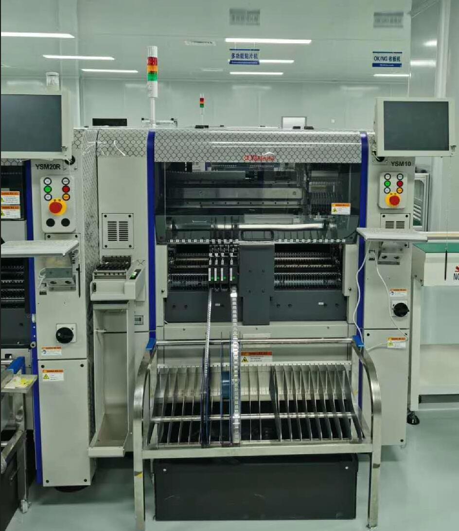
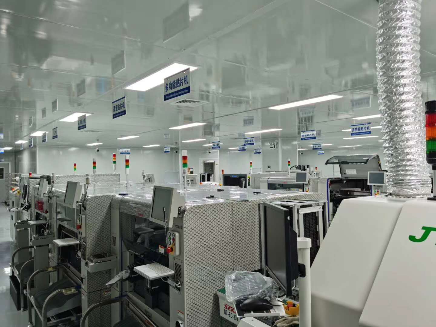
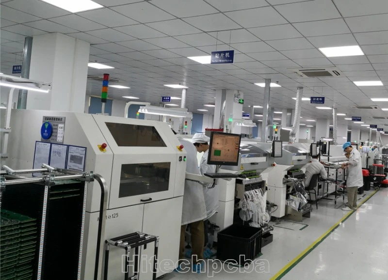
Company Show
Advantages Of Our PCB Design
- Min.trace width 2.5mil,
- Min trace spacing 2.5mil,
- Min vias 6mil ( 4mil laser drilling),
- Max layer count 38 layers,
- Min BGA spacing 0.4mm,
- Max BGA Pin 2500pin,
- HDI highest Layer count 18 layers,
- Fastest delivery time 6 hours per item.

LED PCB Design
What are LEDs PCB board and LED PCB designs?
LED is an acronym for light emitting diode, which is semiconductor diodes. The LED is soldered to the printed circuit board and features a chip that creates the light as electrically connected. A thermal heat sink and a ceramic base are used to bond the chip. Needless to say, LED PCB is the core of LED lighting, and an LED PCB is easy to create a high volume of heat, but making it hard to cool with traditional methods. So metal core PCB is widely used in LED application because of their enhanced ability to dissipate heat, especially aluminum is often used to fabricate PCB for LED lights. In general, the aluminum PCB contains a thin layer pf thermally conductive dielectric material that can transfer and dissipate the heat with much greater efficiency than a traditional rigid PCB.
Now SMD packaging type is the most widely used packaging form in LED applications. In general, it’s limited for the light emitted from a single LED component. So multiple LED components would be used for a single light fixture to achieve sufficient light. Like other semiconductor devices, PCB is the best method to electrically connect the LED components. And a PCB with LED components soldered is usually called as “LED PCB”.

The advantages of LED PCB
With the electronic products is more and more smaller and thinner, making it popular to use LED PCB, and there are various advantages with using LED PCB as follows:
· Lightweight, low profile
· dimensional stability
· thermal expansion
· heat dissipation
· Lower cost backlit membrane switch
· Dust and moisture resistant
· Make it easy to integrate into complex interface assemblies
· Efficient low power consumption
· Available in a wide variety of sizes, colors, and intensities
· May be used in silver flex membrane switches and copper flex membrane switches.
There are two main reasons which make the LED PCB be popular in addition to increasing the light output of the fixture with integrating multiple LED components.
1. It’s easy to tune the color function by integrating the LED components with different color temperatures or different colors into the same PCB.
2. It can achieve the various light fixtures to meet different lighting requirements with the boards that have different shapes, sizes and materials.
The LED lighting industry
LED lighting or light emitting diode is an increasingly popular lighting solution, so it’s popular to improve longevity and reduce environmental impact. There are some benefits of LED lighting for traditional methods as follows:
Lower power consumption: great LED lights with high quality can be six to seven times more efficient than traditional incandescent lights. On average, switching your home from incandescent lighting to LED lights can cut your energy use by more than 80 percent.
Longer Lifespan: LED light bulbs can have a life of over 25,000 hours, or three years of 24/7 use, which is 25 times longer than any traditional light bulb. So it saves you the time, money and effort involved in purchasing and installing new bulbs.
More Efficient: Traditional incandescent light bulbs release 90 percent or more of their energy as heat. LED lights cut this by up to twenty percent. It means more of your energy is going into lighting your home, and less into unnecessarily heating it.
Very Compact: LED lights have various sizes and types in applications due to their small size. It means manufacturers can insert LEDs into anything from computers and smartphones to cars and traffic lights.
Mercury Free: LED lights contain no mercury, unlike more traditional options. So LEDs have a smaller environmental impact than traditional bulbs and can be more easily disposed of, without special disposal procedures.
The application of LED PCB
PCB LED lights have excellent energy efficiency, low cost and maximum design flexibility, so it can be incorporated into numerous lighting applications.
Telecommunications: LED indicators and displays are always used in telecommunications equipment due to the surrounding machinery, and they have great heat transfer ability. Therefore, aluminum-based LED PCBs make a useful effect on their application.
Automotive: aluminum PCB LEDs also are used for cars on indicators, brake lights and in headlights, as well as other applications. There are some factors making the aluminum PCBs be ideal within the automotive industry, such as the durability and competitive prices.
Computer: LED displays and indicators are more and more popular in the computer applications. And aluminum PCB LEDs are an ideal solution because of the heat sensitivity of computer machinery. Expect for LED applications, aluminum PCBs are also used for the computer parts like power devices and CPU boards due to their ability to dissipate and transfer heat.
Medical: Lighting tools used in surgeries and medical examinations commonly use high-powered LED lights, and these LED lights often use aluminum PCBs, which is primarily because of the durability and heat transfer capabilities of aluminum PCB LEDs — this makes sure medical equipment is functioning properly regardless of the number of patients cycling through a medical office. Expect for lighting tools, medical scanning technology often uses aluminum PCBs as well.
SMD LEDs in your PCB
There are many devices including LEDs on a PCB using surface mounted components. If the wires are quite thin, through hole components can bend slightly so that it looks cheap from the outside. If making it right to solder the SMD LED, it will be rigid on the board. What’s more, it can also place the SMD LED behind a screen, and cheaper LED that use a bulb will stick out through the packaging. So it can place the SMD LED behind a small screen in your packaging to be cleaner for your device. As you know, many PCBs that contain LEDs are fabricated with multilayer FR-4 substrates, so you need to have a pattern of closely-spaced filled or plated through vias under each component so that it can transmit heat, as well as get to your power and ground layers.
If your LEDs have a small footprint and are surfaced mounted, it can use our vias. Probably there will be a weak solder joint or even tombstoning because it doesn’t fill or plate over the vias and then solder can wick into the vias during assembly, so the reason why it’s better to just use SMD LEDs on an LED lighting array is that the problem with wicking. A single LED with decent power output will not lead to damaging to your board because of undue thermal. However, if you are going to have a system for lighting applications, it will need to suffer from a massive heat for the board that supports your LEDs, and make it hard to cool with traditional methods for the boards. Because the individual LEDs are too small, you can’t really attach a heatsink anywhere, and a heatsink will block the emitted light anyways. Because there is a great demand on thermal, the boards with a metal core are usually used in LED lighting applications due to their ability to dissipate a great deal of heat. In general, aluminum is used for LED lighting applications as the metal core in PCB. What’s more, aluminum is the most metal used as the core among all the possible metal core PCBs. As well as copper and iron are used for metal core PCBs.
LED PCB Design Principles
LED PCBs play an important and almost indispensable role in modern life. Whether it is the toys you play with, or the street lights outside your window, LED PCBs are everywhere. A technology based on the integration of ‘Light Emitting Diodes’ or LEDs onto ‘Printed Circuit Boards’ or PCBs, they are an interesting and almost innovative piece of technology, which revolutionized electronics.
Offering a wide range of advantages such as low cost, high efficiency, structural strength and so on, they quickly found their way into a wide range of applications. Indeed, the technology itself has started to undergo transformations, given the research and development underway to make things better. Coming to the design aspect of these LED PCBs, there are several different aspects that are taken into consideration.
Our IPC qualified engineers use the latest CAD software to design circuit boards that are optimised to be manufactured. The LED PCB design process combines component placement, tracking, material selection and thermal management to achieve electrical connectivity on a manufactured circuit board.
Component Placement – we don’t just throw them on
As tempting as it may be to just throw LEDs and other components on to the board, it is the process of clever component placement that keeps costs down, manufacturing easy (or as simple as possible) and quality high. We always design for optimal: manufacturability, thermal and optical performance - and good placement is the foundation of this. The arrangement of parts can impact reliability, assembly processes, solder joint integrity and testing. Many aspects of LED PCB design are unique to LEDs and generally unknown to the wider electronics industry. LED PCBs need to be designed to constrain LED movement during reflow soldering and track flood-fill needs to be optimized for thermal performance and capacitive coupling for example.
In addition to LEDs, we’re placing connectors, active and passive components, thermistors and more onto LED PCBs whilst considering mounting holes, through vias and optic placement. With so many considerations it’s no wonder PCB design is like solving a puzzle.
We haven’t even mentioned PCB physical size constraints and creepage and clearance tolerances that impact on placement, electrical test requirements (accessibility) and assembly limitations. Suitable clearance between components is required to avoid an over-voltage event on the board. Creepage is the shortest distance between components measured along the surface of the insulation material – clearance, on the other hand, is the distance between components measured through air. The more components there are to place the more difficult it can be to achieve creepage and clearance. Our team consider the material of the PCB, insulation and pollution that could occur when the PCB is in the application, they then apply the relevant tolerances for creepage and clearance for long-lasting performance.

PCB Materials
There are various PCB materials that can be used for LED applications: both FR4 and insulated metal substrate (IMS) are popular choices. Each material has its own relative merits, ranging from cost through to thermal performance.
IMS as a PCB material is comprised of three main elements; a metal base layer, a dielectric film, and a copper top-layer. The metal base layer forms the bulk of the PCB thickness and gives mechanical structure and thermal mass, typically the metal used will be aluminium as it offers good thermal performance versus cost. Not all IMS PCBs are the same, high-performance IMS materials have dielectrics with higher thermal conductivity, which ultimately can yield to a product with significantly longer lifetime.
In summary, IMS PCBs are inherently very good at dissipating heat because they are made almost entirely of metal; however, they are typically more costly than FR4 material
FR4 is what most people think of when you say, ‘PCB material’. It is used widely in all manner of electronics and so it is a very familiar material for designers of circuits. FR4 material is constructed from reinforced resin onto which a copper foil has been mounted. As the resin material is an insulator it is possible to create a laminate of many circuit layers placed one on top of another, interconnected as required. Given the thermal performance of IMS surely FR4 is inferior? Not necessarily. With clever PCB design, it is possible to achieve good thermal conductivity through FR4 materials, essentially creating thermal pathways through the resin that do not impact the electrical functionality of the PCB.

Why use Led PCBs in a design?
LED PCBs have become the go-to choice for many lighting applications for a variety of reasons:
Their lightweight and low profile make them easier to use in modern electronics
LEDs can reduce energy consumption by up to 80%
They’re useful for any industrial lighting application where lighting needs to be resistant to moisture and dust
Their long life makes them attractive to automotive and appliance manufacturers
How easy are led pcbs to design and produce?
Electronics manufacturers need to consider not just the LEDs when constructing the board, but also the other components. How close are the LEDs to other components? Laying out a solid design before production begins keeps board errors low by allowing the proper tolerances between each component.
One of the challenges of designing an LED PCB board is heat dispersal, as LEDs can produce a significant amount of heat. The standard FR-4 board material made of epoxy and glass is not well-suited to transferring heat, which means the LEDs can damage the connections in the board.
A MCPCB is a PCB with a metal core that can transfer heat away from the sensitive components. Aluminum is the most popular type of metal used in these applications.
If you want to mount LEDs to a board, you need to determine which kind of PCB to use. Off-the-shelf modules have already been designed and tested, but full custom designs require careful consideration of the different temperature ratings of the materials and their standards for heat resistance.
The use of LED PCBs must quite an extent become ubiquitous with many applications making use of them. In fact, the use of LEDs in standard printed circuit boards is quite a technological revolution. They offer several advantages including but not limited to:
Low Cost.
High on efficiency in terms of power consumption.
Compact structure including their light weight and small size.
Resistance to dust & moisture.
Improved lifespan, and more.
To avail of the many advantages offered by LED printed circuit boards, however, it is imperative that some key design aspects be kept in mind. Here is a quick look at some of them.
Key considerations in LED PCB design
Component placement
One thing that is crucial when it comes to LED PCB design, it is proper component placement. With the right component placement you can not only ensure easy manufacturability but also ensure quality.
It is important to maintain a certain distance when it comes to placement of components on the board else it can lead to overvoltage. It is therefore important to consider two aspects:
Creepage or the shortest distance between components.
Clearance or the distance between components measured through the air.
It is also important to ensure that the components are not placed near the PCB outline. Placing components towards the edge can lead to dislodging of components.
Also, it must be kept in mind that all Surface Mounted components follow the SMD PCB design rules. Through-hole components similarly must be placed on top of the board so that the number of steps required for assembly, are optimized.
As for blind and buried PCB vias they should not be placed too close to SMT pads as doing that can mean that the solder can migrate away from the pad. In such situations, there is the possibility of a faulty joint. As a thumb rule, therefore, a distance of 0.025 inches or more should be maintained between the vias and the SMT pad.
Aluminum PCB for LED
Aluminum PCBs, when used correctly, are highly efficient, brilliant heat dispensers and provide excellent signal connectivity. The PCB boards mainly consist of Aluminum but might also contain other materials such as silicon, magnesium, and different types of metal. When Aluminium PCB is produced, it has multiple layers, each with its function and use:
The First layer – this layer consist, you guessed it, of Aluminum! As the first layer, it must be solid and durable. The other layers will base on top of the aluminum layer.
The second layer consists of thermal insulation material, a material made out of ceramic polymer. The polymer prevents external PCB damage due to mechanical moving parts or heat dispensed on and around the board.
LED circuit layer, The third and last layer. This layer consists of the custom design layout and schematic wiring. This layer contains mostly copper, similar to other PCB-designed boards.
Thermal management
High temperature can impact the longevity of LED lights. To ensure thermal management, therefore, the following are used to dissipate heat:
Aluminum Cores
Thermal Vias
Heat Sinks
For thermal management it is also important that the right component placement be undertaken.
Tracking
Careful tracking is a prerequisite in order to ensure there are no short circuits or crosstalk. If there is proper trace routing, you can rest assured that there is no interference from other networks. The right track width also goes a long way in preventing overheating. It is also important to pay due attention to:
Tracking Space
Mounting Holes
Finishes
The finish of the board helps in protecting the copper as also offering a soldering surface. Some of the common finishes include:
HASL
OSP
Electrolytic Nickel
Electrolytic Gold
Immersion Tin
Immersion Silver, and more.
The pros and cons of each finish need to be carefully ascertained.
To Sum Up
When it comes to LED PCB, we need to ensure that the following challenges are suitably mitigated:
Heat – The design should ensure that there is optimal thermal management so that longevity is maintained. This is because the temperature of the LED circuit has an inverse correlation with the longevity of the LED.
Color of the light – Once the temperature of the LED circuit increases the colors of the LED can change. Therefore proper heat dispersal is key.
Efficient PCB design, therefore, is a key aspect of manufacturing the right LED solution. It is imperative that you choose the right partner who has the requisite industry knowledge and can also ensure that the PCB designs are customized to the bespoke needs of your applications.
Light PCB assembly
When it comes to LED PCB assembly, there are multiple options. The PCB might have a single or dual layout (single side or double side assembly). The community itself is done by two standard techniques – SMT and DIP:
SMT PCB assembly – SMT stands for Surface-mount and is the most common way to assemble a PCB, and LED PCB is no different. We can archive this by mounting the components on top of the PCB using a pick-and-place machine. Once the details are mounted on the printed circuit board, the PCB is inserted into an oven. The oven will regulate the temperature and safely join the solder paste with the components. An efficient LED PCB assembly machine can paste thousands of PCBs a day. They are making this process highly efficient for mass production.
DIP assembly – called through-hole PCB assembly, DIP components are inserted manually into designated holes. The PCB will then enter a wave-soldering machine that will solder the components in place. This process is less efficient than SMT. It has a higher fault rate due to the manual work involved in placing the details manually.
Hybrid LED PCB assembly – some designs can't be either SMT or DIP and require both. In such a case, SMT will be done first, and the DIP components will be soldered by hand.
Regardless of the assembly technique used during the LED PCB manufacturing process, the LED PCB factories producing the board will ensure the board functions properly by using visual inspection and advanced machinery.
At Hitech Circuits, we are fully equipped to handle your LED PCB manufacturing requirements. With over four decades of experience in delivering high-quality, on-time, competitive price products, you can bank on us for your PCB requirements. In case you have any questions regarding LED circuit boards, please feel free to contact us via email at sales@hitechpcb.com or call us freely.

0086-755-29970700
sales@hitechpcb.com; sales@hitechcircuits.com
2F, Building C, Suojia Technology Park, Hangcheng, Bao’an, Shenzhen, Guangdong, China 518126


