 Chinese
 English
 Russian
 Spanish
 Portuguese
Multilayer PCB Design and Manufacturing
Excellent Quality
- 100+ PCB Design & Layout projects per year
- Outstanding designers with 10+ working experiences.
- 7/24 Live sales & tech support
- 6 hours PCB Layout expedite services
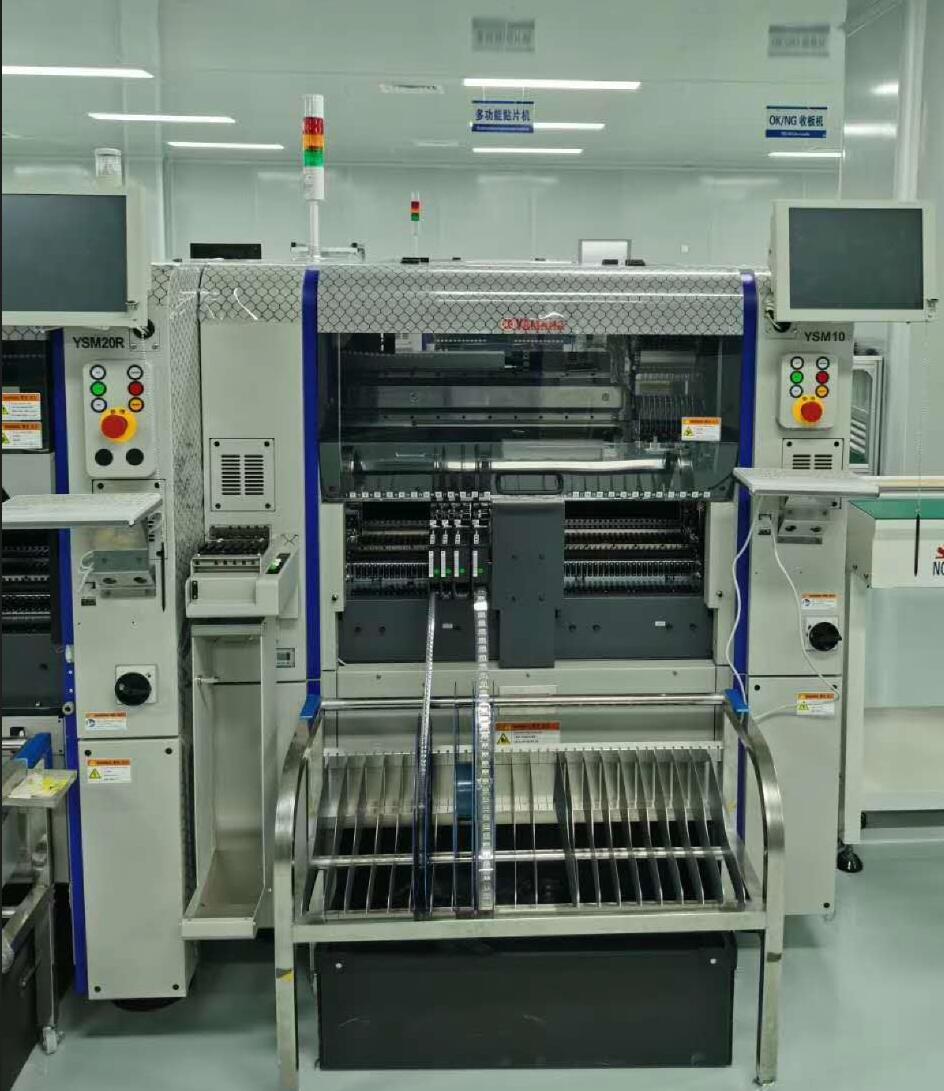
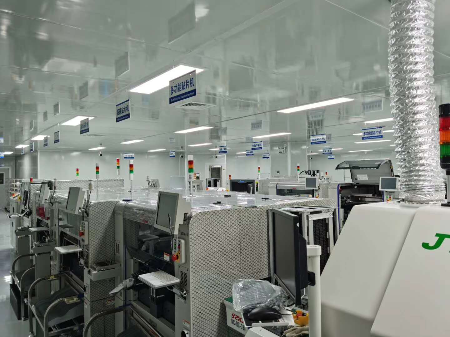
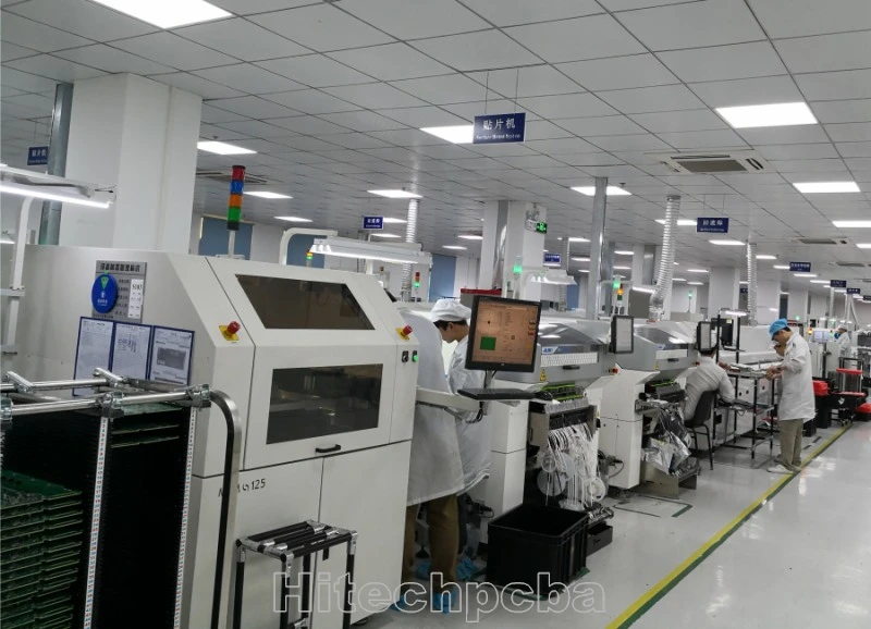
Company Show

Advantages Of Our PCB Design
- Min.trace width 2.5mil,
- Min trace spacing 2.5mil,
- Min vias 6mil ( 4mil laser drilling),
- Max layer count 38 layers,
- Min BGA spacing 0.4mm,
- Max BGA Pin 2500pin,
- HDI highest Layer count 18 layers,
- Fastest delivery time 6 hours per item.

Multilayer PCB Design and Manufacturing
Multilayer PCB Design and Manufacturing
Hitechpcba design team are sophisticated with printed circuit board design and layout services for 10+ years in terms of medical devices, musical instruments, RF converter, smart consumer products, system controllers for solar power, temperature & humidity monitor, IOT units etc.
Hitechpcba can transfer your excellent concept into product quickly as long as you send us requirements (such as functions, shape, drawings etc.). We can complete PCB design and make prototype accordingly. Design job includes schematics, layout, components selection, circuit simulation and software etc. In order to shorten your timeline, we comply with strict standards to handle PCB design phases, such as from requirement draft, alpha & beta review to volume production. In this case, your PCB design tasks go smoothly under our project management team.

Our Products Advantage
1. Over 15 years experience manufacturer in Pcb Assemble and pcb field.
2. Big scale of producing makes sure that your purchase cost is lower.
3. Advanced production line guarantees stable quality and long life span.
4. Design and produce almost any PCB as your requirement.
5. 100% test for all customized pcb products
6. One-stop Service, we can help to purchase the components
Hitech Circuits is capable of providing full turnkey PCB assembly and partial turnkey printed circuit board assembly services. For full turnkey, we take care of the entire process, including preparation of Printed Circuit Boards, procurement of components, online order tracking, continuous monitoring of quality and final assembly. Whereas for partial turnkey, the customer can provide the PCBs and certain components, and the remaining parts will be handled by us.
How to Design Multilayer PCB?
Designing a single or double layer PCB is easy and can be done by any hobbyist with a few components, which are easily available in the market. A DIY article to design a single layer PCB will be available soon.
The multilayer PCB, however, requires skilled engineers to be designed. They use different software’s which are either free of cost or high priced licensed tools and create a lot of predefined rules in the rules section of the selected tool. A good PCB design tool that we use often is Altium Designer, which is easy and convenient to use.
The first and foremost requirement to design a PCB is the circuit layout of the project.Once it is ready, a schematic is drawn using the symbolic library of the PCB software where the components can be found with similar pin descriptions as that in their data sheets. This schematic diagram gives an easy understanding of the components and their connections.
As a professional PCB designer, I have some tips for you, that will help you in designing the multi-layer PCB efficiently.

Always try to add an even number of PCB layers. Since both layers carry signals, the difference in the price segment for odd layers isn’t much. You will also rarely find a manufacturer who produces odd layers at much lower prices.
Choose the right PCB thickness, keeping in mind the number of heavy components on the PCB board.
For example, you can consider PCB with 0.8 thickness if all of the components are lightweight. The thickness support in multilayer PCB design varies with different vendors. However, some standard PCB thickness sizes are 0.8mm, 1mm, 1.2mm, 1.6mm.
Select the PCB stack, as per the design requirements. The PCB engineer selects the method of ground and power planes totally based on the circuit design.
Communicate effectively with the manufacturer and understand the capabilities of the PCB manufacturing.
Cross-check Schematic connections with PCB design and footprints with schematic symbols.
There are ample number of PCB manufacturers available in the market. One of the many factors which affect the cost of PCB manufacturing is the number of layers. Therefore, the cost of production for a multilayer PCB is higher than a single or double layer PCB. This cost increases, as we add more layers to the multi board PCB.
Multi-Layer PCB manufacturing process
Once the design process is finished, the PCB is ready to get manufactured.
This takes me back to the time, when I designed my first multi layer PCB(4 layers) and sent it to a local manufacturing house. I waited for it like a school going kid awaiting his results.I was keen on knowing how the design will turn out to be!
So, yes, Manufacturing stage of PCB is a crucial part of the whole process. It is the time when your design gets a physical form.
In order to send your PCB to the manufacturer, you will need to get the gerber file of the PCB. A gerber file is the standard output file for a multilayer PCB, inbuilt in any of the softwares you choose for your design.
Check if there is an issue with minimum trace width or minimum copper clearance or that the minimum hole size criteria matches or not. If you detect any such issue, you might have to edit it to reproduce the PCB.
The manufacturing process consists of laminating inner different copper layers with prepreg and the dielectric material. The lamination process is done under high temperature and is very critical as the PCB holes need to be matched. A minor difference of layer placement in manufacturing causes noise or even short circuit in PCB, therefore, this process needs to be done with high accuracy. It also takes care of trapping any air bubble so the PCB layers are tightly glued together with epoxy chemicals (industrial glue). The popular materials used for the lamination process are basic epoxy glass, exotic ceramic, and Teflon materials.
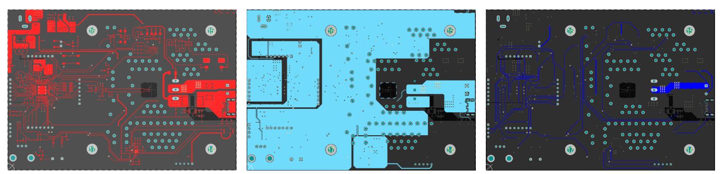
The two images given below will give you a more clear idea about the masking layer of PCB. The masking layer can be of any color depending on the choice of PCB manufacturer. The green color is popular for most of the PCB boards.
The silk layer is written on to the masking layer on the Multilayer PCB board. It is useful to label or designate the components to identify their location on the circuit. It is also used in putting the “LOGO” of any company on board, IC pin identifier mark, and many more things.
The core (dielectric material to separate two layers), and prepreg basically have the same meaning. The core has high width when compared to the prepreg. Both the materials need high temperature and pressure to melt and settle in the required area. After the lamination process, “Masking “ layer is applied on both sides of the multilayer PCB, which prevents our touch on copper lines/traces which can cause ESD to the relevant component. It also provides protection against oxidation and prevents solder bridges from forming between closely placed solder pads.
Multilayer PCB Manufacturers
I thought to list a few of the best pcb manufacturers who have capability in making multilayer printed circuit boards.
Hitechpcba – is one of the top manufacturers of multilayer PCBs. They have a global supply chain and they deliver all over the world. You can upload the designs online using their web app, and you need to place the final order only after getting the right quote.

Quote of PCB Design services
Basically, custom PCB design is related with many factors impacting the cost. After a kickstart and evaluation of circuit board functions, our sales engineer will work with you to make and confirm quote including design, prototype and maintenance during life cycle. Customer just need to write a document of concept, function descriptions, testing and other technical requirements, then send the document to us to get an instant quote.
Multilayer PCB Benefits & Disadvantages
Let’s first go through the benefits of designing a multi layer pcb
Compact Size: One of the major advantages of using a multilayer PCB is that the product/project becomes compact in size. If you are having fun with your smart-phone or having a calorie count in your smart-band or smart-watch thanks to multilayer PCB design to make it really compact.
Increased Flexibility: Multi-layer PCB can be flexible which increases user satisfaction for the end product. There are a number of applications of the flexible PCB like smart watches and smart bands.
Less Noisy: The RF designs which include antenna of 433MHz to 2.4GHz, the high-frequency signals and high-speed signals (clock signals), require a good grounding shield. However, a double layer PCB with a high number of components on board fails to provide a good ground shield for most RF-based designs. The multilayer PCB board, on the other hand,allows the user to place separate ground and power planes so that RF components can have a good ground shield. Also the other components have less return path for ground which results in less noise or noise-free PCB board.
High Quality: The multilayer PCB uses high-quality materials for the process of manufacture and production. Therefore, the fabricated PCB works safely in high-temperature conditions.
Impedance Control: Several communication protocols like USB, SPI need to be routed to the tracks with the relative impedance of the track. For example, the USB D+ and D- lines need to be controlled with 90 OHM impedance with respect to ground, length matching for all the nets of SPI is also required. For impedance to be controlled, the separately defined ground plane in the multilayer PCB is very useful. For antenna feedline 50 OHM impedance is needed to be controlled. This can also be achieved by multilayer PCB design easily.
Ease of Design: Lower number of layers increases the complexity of PCB design when the space is limited for circuits that require numerous components on board. With multilayer, the number of layers can be added to ease the design process and reduce the efforts in finishing the design.
Disadvantages
The Multilayer PCB has some disadvantages as well. Some of the major drawbacks have been discussed below:
Expensive Manufacturing: Right from its design to the manufacturing, the multilayer PCB has at every step this multilayer PCB board deals with more complex processes when compared to the single or double layer designs. Since it requires a highly complex and accurate manufacturing process, the time and labor work as well as machines for the lamination and epoxy materials comes out to be a bit expensive . Integrating each layer with accuracy is the biggest task to be completed. The use of blind and buried viasmay also further add to its cost. (Blind and Buried Vias are used to route signals and expose “via” through the selected layers only).
Designing Skills: The designer should have enough knowledge and idea of multilayer design, along with a better idea about impedance control, ground shielding, and good layer stack design. The fees for a multilayer pcb designer are more compared to a double side-board designer.
Test and Debug: The increased complexity comes with increased difficulty in testing the multilayer design, as users can not cut track if the track is somewhere any layer inside multilayer board, unlike a single or double layer PCB.
Manufacturing time: The manufacturing process of Multilayer PCB is time taking owing to the fact that the production processes need to be performed with the right accuracy.
Limited manufacturers: The production process requires high accuracy and very expensive machines, therefore only few manufacturers who support the multilayer board production process are available. This limits the choice to select a manufacturer to produce the multilayer board.
Multilayer PCB Applications
The multi layer PCB finds its uses in a wide range of applications. Some of them are listed below:
Consumer Electronics
Consumer electronics have the biggest market of multilayer PCB boards.
Some of the trending wearable gadgets such as the smart-band and smart-watch, Smart TV, Voice recognition gadgets like “Amazon Alexa” and “Google home”, Smart home products and so on. The smartphone you are holding currently while reading this article also has a precisely designed and accurately manufactured multilayer PCB inside.
Industrial Electronics
The well-known mass production houses of almost any electric or non-electric company have automated robotic machines to produce in bulk. They use multilayer PCB boards in the machines to make it compact and to add more features in a limited size.
Medical Electronics
The day is not far when the programmed robots will do the surgery of humans, the number of devices from heart rate monitoring to HCG monitoring and even blood pressure monitoring devices are now automated, all credits to multilayer boards.
Apart from this, there is a lot of sectors where multilayer PCB boards are being used as,
Telecommunication
Satellites
Automotive
Cloud computing
Atomic and nuclear stations
Navigation systems
Our project manager follows up the whole design process, which enables you know every single detail of PCB design (if necessary). Meanwhile, we will build an online document. Through interactive editing and confirmation, design job will be expedited than you imagine. Let’s work together to fulfill your market goal by our fast & safe PCB design services.

0086-755-29970700
sales@hitechpcb.com; sales@hitechcircuits.com
2F, Building C, Suojia Technology Park, Hangcheng, Bao’an, Shenzhen, Guangdong, China 518126


