 Chinese
 English
 Russian
 Spanish
 Portuguese
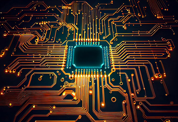
PCB Design & Layout
Hitech PCB Design & Layout
PCB Design Board Manufacturer & Assembly – One-stop service
Hitechpcba can transfer your excellent concept into product quickly as long as you send us requirements (such as functions, shape, drawings etc.). We can complete PCB design and make prototype accordingly. Design job includes schematics, layout, components selection, circuit simulation and software etc. In order to shorten your timeline, we comply with strict standards to handle PCB design phases, such as from requirement draft, alpha & beta review to volume production. In this case, your PCB design tasks go smoothly under our project management team.
Hitechpcba has the full selection of design software, such as Cadence Allegro\ORCAD, Mentor WG\PADS, Protel99\ Altium Designer (AD)..etc. Please let us know which EDA tools you want use in your project, our most frequently used software are Eagle, Altium Designer, Protel( protel pcb design), PADS.
When you are the wiring, the first time needs to finish some important, several signal lines, such as DDR, HDMI, Network Port, TUNER, Panel, CA, USB, Audio and Video and so on. you can fine-tune the layout then get traces are as smooth as possible.
Excellent Quality
- 100+ PCB Design & Layout projects per year
- Outstanding designers with 10+ working experiences.
- 7/24 Live sales & tech support
- 6 hours PCB Layout expedite services
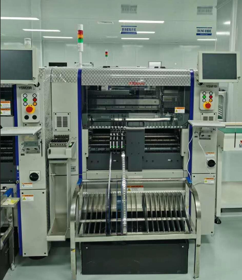
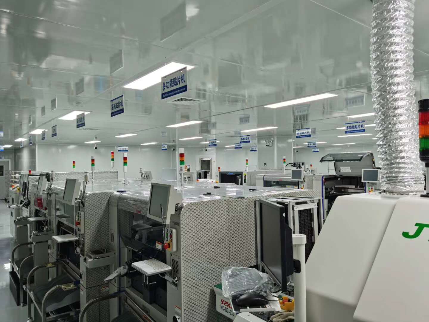
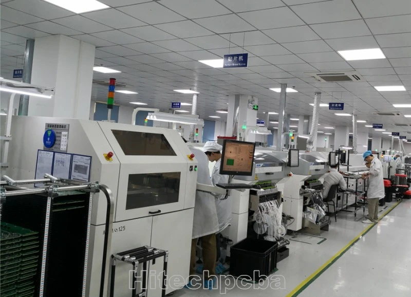
Company Show
Advantages Of Our PCB Design
- Min.trace width 2.5mil,
- Min trace spacing 2.5mil,
- Min vias 6mil ( 4mil laser drilling),
- Max layer count 38 layers,
- Min BGA spacing 0.4mm,
- Max BGA Pin 2500pin,
- HDI highest Layer count 18 layers,
- Fastest delivery time 6 hours per item.
PCB Design & Layout
What is PCB Design and Layout?
PCB design and layout is the process of creating the physical layout of a printed circuit board, which is used to connect electronic compo-nets in a circuit. The process involves designing the placement of electronic components, routing the electrical connections between them, and defining the shape and size of the board. Hitech Circuits provides a full scale of printed circuit board design services, with a highly experienced design team that specializes in all kinds of printed circuit board design, from simple to complex.
We provide reverse engineering services with PCB Design and full Gerber Data generation from your sample PCBs as well.

PCBA Electronic Manufacturing Services
Primarily concerned with PCBA we offer a wide range of services relating to electronics manufacturing. You can engage us at any stage of your project from schematic design through PCB design to mass production. If needed, we will do research and development to produce your first PCB prototype as happily as we would do it from your own circuit board design.
Talk to us about your project, schematic design or PCB design and our expert staff will provide the benefit of their experience in both designing our own products and assisting other companies with bringing their products to production. Whether we do your schematic design to develop the best design for you, or you have a complete PCB design ready for production already, we can help you bring it to final PCB assembly runs of any amount required.
Our experienced staff can advise on electronic parts selection and availability either from a schematic or a BOM. Whether you require surface mount technology, through hole or a combination of both, we have the experience to bring your design from the concept stage through to mass production. We can take care of mechanical assembly as well, inclusive of designing parts for moulding.
Our qualified professionals can offer you service and technical support to produce a polished product at a price that meets your budget. Take a look at what we have to offer before you commit with anybody.
Our PCB Design and PCB layout's Capabilities:
Double Sided & Multi layer PCB Designs
Radial Layouts and Non-standard Geometries
High frequency RF / Microwave PCB designs
High Speed PCB board
High Density board/ HDI PCB boards
Flexible PCB boards
Heavy copper PCB/ Power PCB board
Design Tools
Gerber, drill files & PCB File
Assembly and fabrication files
Formal drawings on customer format
Gerber, drill files & PCB File
Assembly and fabrication files
Formal drawings on customer format
Welcome to send your enquiry to sales@hitechpcb.com
Find a PCB Design Company and vendor. Choose Quality PCB Design company, Suppliers at hitechpcba.com.

PCB Design Tools
Allegro, Pads, Mentor Expedition, Altium Designer
PCB Design Package Types
BGA, uBGA, CSP, QFP, QFN, TSSOP, TQFP, SOIC
PCB Design Schematic
CIS/ORCAD, Concept-HDL, Montor DxDesigner, Design Capture, etc.
Hitech Circuits believes in courteous, swift and professional customer service. The company’s goal is to provide rapid and high-quality solutions to the satisfaction of all customers – both new and old. Many years of experience, use of advanced technologies, compliance with the requirements of IPC standard, and a team of highly experienced and knowledgeable designers that plan every step in advance.
PCB Design - With varied production technologies
RIGID Multilayer / Motherboards/Backplanes / All Types IAW IPC2221+IPC2222
Flexible / Rigid-Flex PCBs In-Accordance-With IPC-2223
MicroVias / Stacked & Staggered & Blind & Buried Vias IAW IPC2226
HDI= High Density Interconnect IAW IPC2226
PCB Design Capability
Highest layers::38 Layers
Maximum PIN count:69000+
Maximum connections:55000+
Minimum line width:1.5mil
Minimum line spacing:1.5mil
Minimum via:6mil(3mil laser hole)
Maximum BGA in a single PCB:62
Maximum BGA PIN spacing:0.4mm
Maximum BGA PIN count:2597
Highest speed signal:28Gbps
HDI PCB design: 1+N+1, 1+1+..+1+N+1+1+..+1, M+N+M Stacked Microvia and Any layer HDI PCB up to 30 layers.
Required information to quote pcb design & Layout
Complete and verified schematic(s) in one of the software platforms we offer: PCAD, Cadence Allegro, PADS (Mentor Graphics), or Altium Designer.
Complete and verified BOM. Customer must spec. out each component for the layout, based on their familiarity with requirements of the circuitry.
Part numbers for components must be complete, along with package/footprint details for each component.
Board form factors (Dimensional details, board thickness, tooling hole locations, mechanical constraints, etc.) in one of the software platforms we offer, listed above. We can also work with DXF files from CAD tools (like AutoCAD, etc.). Also provide details on: surface finish, solder mask, silkscreen, finished copper weight, etc.
Any special layout routing or fabrication requirements. Special Requirements or Non-Standard Tolerances.
Is the board to be RoHS compliant, Yes or No?
What is PCB Design?
The layout design of a printed circuit board is a significant element to be considered when designing any electronic product. The designer of the PCB layout plays the major role in the electronic circuit design. He or she also takes out the design and layout of the PCB from a specific schematic.
The PCB design and layout is a great skill that requires some knowledge of the software. The software you must gain some knowledge on includes the CAD system, coupled with other techniques. The standards used will ensure that the circuit board is transferred successfully to the PCB. This also ensures that the PCB manufacturing process is successful.
To achieve this success, there are guidelines you must follow. However, we have experts that have the necessary experience and can handle the design without any guideline. Regarding PCB production, there are different softwares available. It is advisable to choose one that most people involved in PCB design prefer using.
Softwares people use for PCB board design include Cadence Allegro, Altium, PADS, and Xpedition. Some of these softwares handles the job better than others.

PCB Design Types by materials
Depending on the application, there are different PCB designs you can pick from. Please continue reading to learn more.
Flex PCB Design
This PCB design can be bent at different angles. Whatever material you are using when making flexible PCB must be bendable round different corners. A flex PCB design’s main materials are copper and substrate materials that are flexible. These are combined making use of adhesives, heat, and pressure.
The substrate utilized by many manufacturers is polyimide. This thermosetting polymer is strong and flexible. Polyimides that can be utilized are Apical, Norton TH, UPILEX, Kapton, Kaptrex, and VTEC PI.
Rigid Flex PCB Design
From the name, this refers to a PCB having a flexible and rigid circuit working together. This design is significant because it has advantages of the flexible and rigid circuits. Most of the PCB components are carried by the rigid circuit, while that flexible part serves as the connections.
This flexible section serves space and weight and is usually found in portable devices like cell phones. Asides from this, it also assists in reducing the complexity of the packaging. It achieves this by eliminating the need for interconnect wirings.
Multilayer PCB Design
This is a PCB design having three or more layers. Its conductors have more than three layers, and are usually found at the middle of the material. This component is very important in aerospace PCBs. This can also be found in applications like file servers, computers, cell phone transmitters, data storage, and repeaters.
It is also useful in applications like atomic accelerators, fire alarm control, space probe equipment, and equipment for weather analysis.
Using this PCB design is beneficial because of its smaller size, easy incorporation, increased flexibility, and reduced interconnections.
High-Speed PCB Design
This PCB design has to do with interrupting equipment signals. This is made possible by the circuit board’s physical characteristics like interconnections, layout, and packaging.
It has to do with issues like emissions, delays, or crosstalk whenever the designing of these boards is initiated. This design is one of the most distinct due to the type of attention it gets. It can be used in designing a board where component placement and routing is the main focus.
High Power PCB Design
One very important rule you must adhere to is to know the Printed circuit board’s power path. The circuit’s location and amount of power is another important consideration when working with high power designs.
Asides these factors, other factors to look at include the ambient temperature that results around the design and the board, the amount of power flowing through the circuit, the airflow around the device and the board, and the density of the board’s IC, and the material used to make the board.
HDI PCB Design
This is one fast-growing technology for PCB designs. The HDI PCB has microvias and blind and/or buried vias, which usually have a thickness of about 0.006 micrometres.
This board’s circuitry density is higher than PCB’s normal densities. HDI boards come in six types. These include:
A board having both through and buried vias
A through vias that extends through different surfaces
Multilayer interconnect with high density that has through vias
HDI PCBs coreless construction making use of layer pairs
A HDI PCB alternate construction utilizing layer pairs
Passive substrates that lack electrical connections
Using this PCB comes with some benefits. These include:
It allows the placement of more components on both sides of the PCB
The manufacturer can place components that are smaller very close to others
The reduction in the size and pitch of the components permits an increment in I/O
Allows signals to be transmitted quickly and also reduces loss of signal and crossing delays significantly
LED PCB Design
This is called Light Emitting Diode PCB design. This is a great development in LED lighting technology. It has to do with connecting the LED to a chip delivering light and the circuit board whenever there is a flow of electric current.
The chips can be bonded by using thermal heat sinks and ceramic bases. It generates very high heat. This is why it is difficult to cool it using traditional methods. Therefore, you’ll look for metal cores due to their ability to release heat. Aluminum is a common metal found in LED PCBs.
Aluminum PCBs feature a thin layer made up of a dielectric material, which can conduct the heat needed. Through it, heat can be conducted and transferred from the system, which makes it better compared to the traditional PCBs
Due to their great abilities, the LED PCB design is useful in different applications.
LED PCBs can be used in applications such as street lighting, airport runway lighting, medical lighting applications, and automotive headlights. Other applications include solar or photovoltaic lighting, highway tunnels, traffic and signals lighting, and flashlights and lanterns. LED PCBs can also be found in hospital lightings like operating or theatre rooms, lightings for growing plants, and more.
RF PCB Design
This is called radio frequency printed circuit board designs. This is seen as one of the most exciting pieces that engineers have worked on.
You will most likely find boards with high-frequency in technological inventions to come soon like sensors, robotics, and smartphones.
This design’s high complexity makes it a very difficult one to develop. The printed circuit boards’ industry will categorize any 100MHz functioning PCB as a radio frequency PCB. Devices making use of RF PCBs are usually complex and can work with both digital and analog signals. Some devices can accept different configurations of about 50 layers.
High Voltage PCB Design
This electric board design is well-known in applications requiring extremely high voltages. You must have suitable clearances and enough space when designing high voltage PCBs. This helps in getting rid of any electrical arcing or breakdowns.
When coming up with high-voltage PCBs, you should consider some things. These include creepage distance, clearance, altitude, basic insulation, double insulation, functional insulation, supplementary insulation, reinforced insulation, and basic insulation.
The clearance and creepage is affected by the PCB type, environment, altitude, and the insulating material grade.
Amplifier PCB Design
Amplifier PCB Designs are most likely found in devices producing sound. It has been a challenge designing a fully functional audio circuit due to its complex nature. Therefore it is important you have a layout to follow while designing the PCB.
Some factors to consider before designing your amplifier PCB design includes:
The power supply, as well as the grounds for it where transformers stand out
Interfacing must be done in line with the layout of the amplifier PCB design
Op Amp circuits which helps in the audio signals inversion in achieving simple circuits
Capacitors from which the audio signals will pass through
MCPCB Design
This is referred to as Metal core PCB. These boards utilize metal as their base material in spreading the heat. These metals serve as alternatives for FR4 and CEM3 boards. This is because it allows better and faster dissemination of heat. Metal core spreads the heat to some other areas like the heatsink backing and the metallic core.
The material used in making MCPCB varies. The most common of them include copper, aluminum, or mixtures of alloys made of metals.

0086-755-29970700
sales@hitechpcb.com; sales@hitechcircuits.com
2F, Building C, Suojia Technology Park, Hangcheng, Bao’an, Shenzhen, Guangdong, China 518126


