 Chinese
 English
 Russian
 Spanish
 Portuguese
High Speed PCB Design
Excellent Quality
- 100+ PCB Design & Layout projects per year
- Outstanding designers with 10+ working experiences.
- 7/24 Live sales & tech support
- 6 hours PCB Layout expedite services
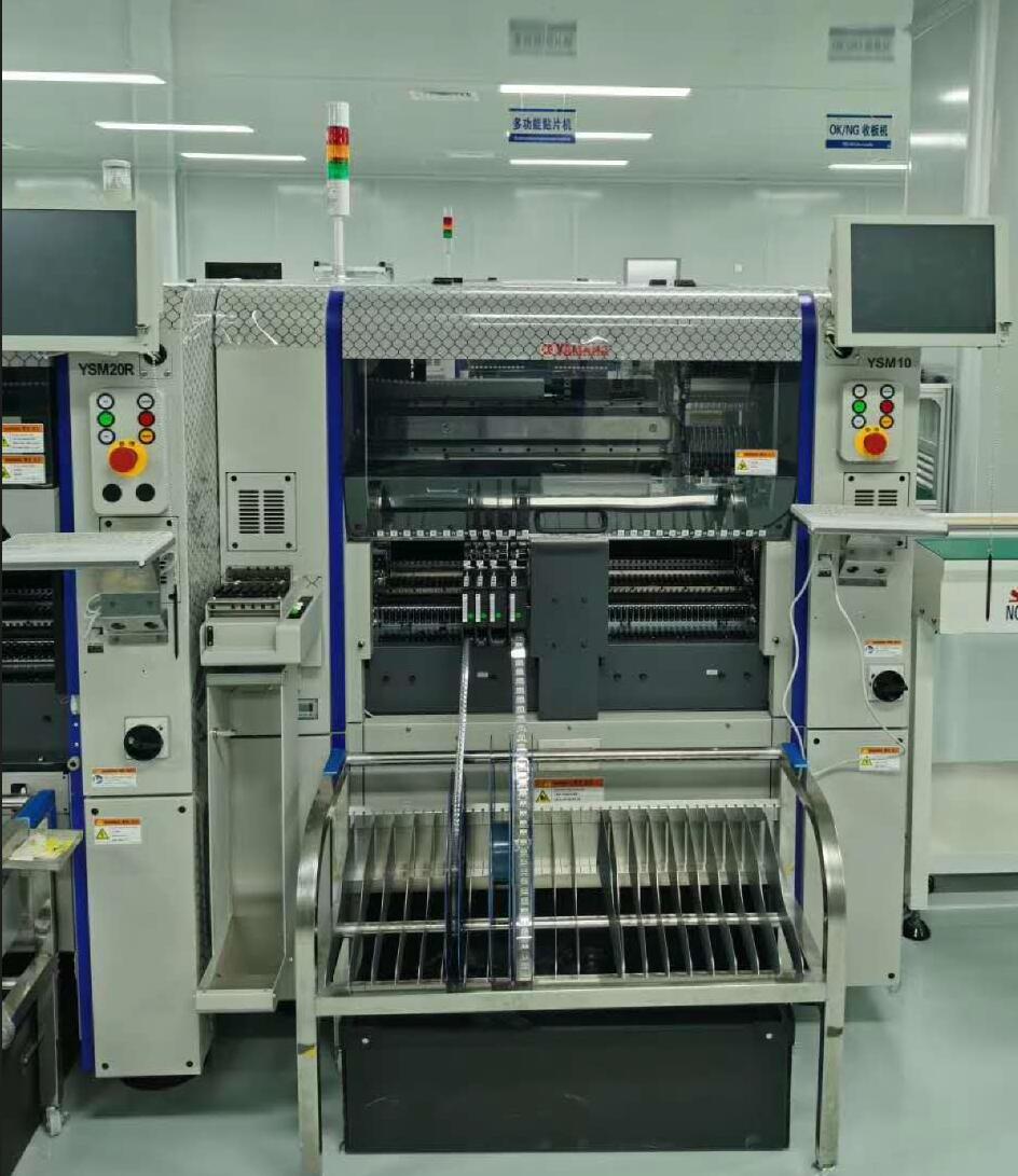
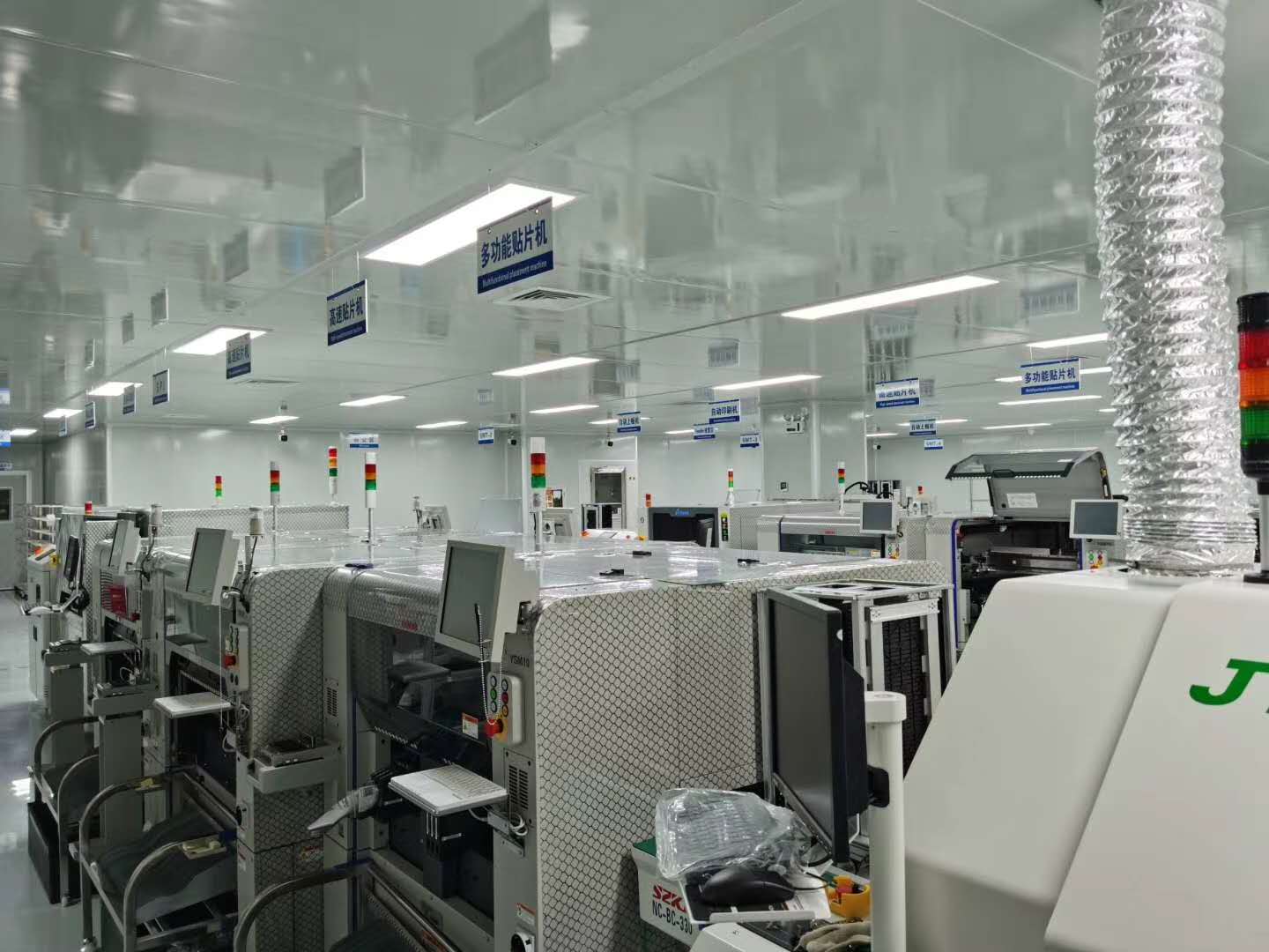
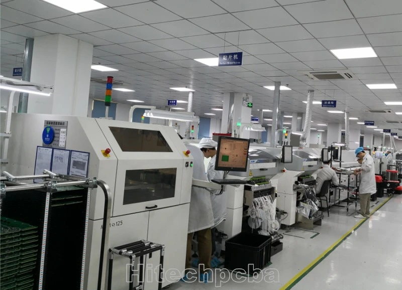
Company Show

Advantages Of Our PCB Design
- Min.trace width 2.5mil,
- Min trace spacing 2.5mil,
- Min vias 6mil ( 4mil laser drilling),
- Max layer count 38 layers,
- Min BGA spacing 0.4mm,
- Max BGA Pin 2500pin,
- HDI highest Layer count 18 layers,
- Fastest delivery time 6 hours per item.

High Speed PCB Design
High-speed PCB design guidelines
In the PCB design, it is generally considered that if the frequency of the digital logic circuit reaches or exceeds 45MHZ~50MHZ, and the circuit operating above this frequency has already occupied a certain amount (for example, 1/3) of the entire electronic system, then it is called high speed circuit.
High-speed PCB design is developed with large-scale improvements in system design complexity and integration, because when the system is operating at 50MHz, transmission line effects and signal integrity problems will occur, and when the system is operating up to 120MHz unless high speed is used. Circuit design knowledge, otherwise the PCB based on the traditional method design will not work. Therefore, high-speed circuit design technology has become a design method that electronic system designers must adopt.

High-Speed PCB Design in Hitech Circuits
High-speed printed circuit board design is a process of balancing the circuit design requirements, device technologies, and fabrication materials and methodologies, to deliver a PCB that can transfer signals between the components, with integrity.
After many years of research and practice, Hitech Circuits can well meet the requirements of high-speed PCB design. We can provide you with high-quality, fast PCB design for high-speed, high-density, digital-analog hybrid, and PCB design of new processes and new technologies (such as flexible boards, HDI PCB, buried blind holes, etc.). We have a group of high-quality PCB design engineers in Shenzhen. We have rich experience in carrier-class high-speed multi-layer circuit board PCB design. We comprehensively consider timing requirements, stripline and microstrip, signal matching scheme, Signal quality, signal trace topology, power ground decoupling, high-speed signal return current return path signal impedance control and stack stackup control, single-board EMC/EMI policy analysis, blind via and buried via and so on, and from the perspective of high-speed pcb layout, use our experience to optimize your schematic design so that your board's inherent quality is higher and the operation is more stable.
Are your PCB Layout High-Speed?
More and more PCBs combine multiple circuits. Your PCB doesn’t have to clock at gigahertz to be high-speed – and to add to that, technologies like IOT and smart home controllers are growing exponentially.
Even using standard components like DDR3, DDR4 or DDR5 SDRAMs means following high-speed PCB design guidelines. You need to constrain your PCB layout to achieve top-class signal integrity – so it works properly – but also so your product is the best it can be.
eCADSTAR isn’t the only solution that lets you do that. The difference is in the way it’s all built-in, not an afterthought – and its unrivalled ability to work with the complex detail you need for ultra-critical layout.
But before we delve into details, what key high-speed constraints do you need?
High-speed PCB design is a very complex design process. Many factors need to be considered in the design. These factors are sometimes opposed to each other. For example, if the high-speed device is placed close to the layout, the delay may be reduced, but crosstalk and significant thermal effects may occur. Therefore, in the design, we weigh the various factors and make a comprehensive trade-off consideration: not only meet the high-speed PCB design requirements, but also reduce the complexity of the design. Our adoption of high-speed PCB design tools constitutes the controllability of the design process. Only controllable, it is reliable, it will be successful.
Elements to Consider
The process of routing a board with high-speed signals requires you to manage:
Termination components that may be required
The definition of the signals that need high-speed design rules applied to them
The mechanical dimensions of the routes - for controlled impedance routing
The properties and dimensions of the board materials
The quantity and arrangement of the layers in the layer stack
The return path of each high-speed signal
The impact and configuration of vias
The configuration and routing of differential pairs
Configuring and controlling the route lengths
Pre- and Post-layout Signal Integrity Analysis
Early in the design process, it is important to identify signals that might require impedance matching so that additional termination components can be included before the component placement process is complete. Since output pins are typically low impedance and input pins are typically high impedance, termination components may need to be added to the design to achieve impedance matching.
Hitech Circuits includes a signal integrity simulator that can be accessed during both the design capture and board layout phases of the design process, allowing both pre- and post-layout signal integrity analysis to be performed (Tools » Signal Integrity). The signal integrity simulator models the behavior of the routed board by using the calculated characteristic impedance of the traces combined with I/O buffer macro-model information as input for the simulations. The simulator is based on a Fast Reflection and Crosstalk Simulator, which produces very accurate simulations using industry-proven algorithms.
Because both design capture and board design use an integrated component system that links schematic symbols to relevant PCB footprints, SPICE simulation models and signal integrity macro-models, signal integrity analysis can be run at the schematic capture stage prior to the creation of the board design. When no board design is present, the tool allows you to set up the physical characteristics of the design, such as the desired characteristic trace impedance, from within the signal integrity simulator. At this pre-layout stage of the design process, the signal integrity simulator cannot determine the actual length of particular connections so it uses a user-definable average connection length to make its transmission line calculations. By carefully choosing this default length to reflect the dimensions of the intended board, you can gain a fairly accurate picture of the likely signal integrity performance of the design.
Nets with potential reflection problems can be identified and any additional termination components can be added to the schematic before proceeding to board layout. The values of these components can then be further tuned once the post-layout signal integrity analysis has been performed.
Defining the High-Speed Signals
High-speed design is the art of managing the flow of energy from one point on a circuit board to another point. As the designer, you need to be able to focus your attention and apply the design constraints onto a signal that travels from this point on the board to that point on the board. This signal you are focusing on is not necessarily a single PCB net though. The signal might be one branch of A0 in a design that you intend to route in a T-branch topology, with the other branch of A0 being another signal you need to focus your attention on as well, and be able to compare the route lengths of these two signals. Or the signal might include a series termination component in its path (which the PCB editor sees as one component and two PCB nets), and if that signal is in a differential pair, its length needs to be compared to the length of the other signal in that pair.
You can manage these requirements using a feature known as xSignals, where an xSignal is essentially a user-defined signal path. You select the source pad and the target pad (in the workspace or in the PCB panel) then right-click on either to define that signal path as an xSignal. As well as interactively defining an xSignal by its start and end pads, you also can run the intelligent xSignals Wizard, whose heuristics will help you to quickly set up a large number of xSignals between the chosen components. These xSignals can then be used to target design rules to your high-speed signals. The software understands the structure of these xSignals; for example, calculating the overall length of multiple nets connected through a termination component, as well as the distance through that termination component.
The PCB panel includes an xSignal mode that is used to examine and manage the xSignals. The panel also provides feedback on the signal length, highlighting xSignals that are close to meeting (yellow) or failing to meet (red) the applicable design constraints. In the image below the xSignal lengths of the CLK1 differential pair are different in length by more than allowed by the applicable Matched Length design rule. The panel includes the Signal Length, which is an accurate point-to-point length. Traditional length inconsistencies, such as tracks within pads and stacked track segments, are resolved, and accurate via span distances are used to calculate the Signal Length.

How to design a high speed PCB!
It wasn’t that long ago when the word “high speed” didn’t exist in the vocabulary of PCB designers. Thinking back for example at the 90’s and 00’s, the speeds they used were much slower. In 2005, 3 Gbps was considered the typical high speed data rate, but today engineers are dealing with 10 Gbps, or even 25 Gbps.
It wasn’t that long ago when the word “high speed” didn’t exist in the vocabulary of PCB designers thinking back for example at the 90’s and 00’s, the speeds they used were much slower. In 2005, 3 Gbps was considered the typical high speed data rate, but today engineers are dealing with 10 Gbps, or even 25 Gbps. In the past the concern was all about putting the puzzle pieces together and strategizing your way through a physical board layout. But how about a high speed design? Now there’s a bunch of invisible forces to worry about, things like electromagnetic interference (EMI), crosstalk, signal reflection, weave of the PCB material and the list goes on and on. Here we discuss a couple of design tips to bear in mind when you are designing ahigh speed PCB.
Start Your High Speed Design Process With a Plan
Without a plan and a strategy for your high speed design project, you’ll likely encounter setbacks and unexpected issues. So before even laying down a symbol or connecting a net, you need some kind of a checklist in hand of what you can expect and what you want as a end product.
Document Every Detail of Your Board Stackup for Manufacturing
It’s important that you use enough time to define and document your layer stackup requirements thoroughly. This is a perfect moment to get together with your manufacturer to determine which materials or IPC spec you should use for your board, and which specific design rules you should follow. We have many customers who we help at the start of a project to guide them in the correct way, so they have the best starting point for a PCB which can be produced while having thought about the cost and quality drivers. IPC-4103 specifies materials for High Speed PCB.
High Frequency Applications. Underneath some examples:
FR-4
This is a great material when you’re working with clock speeds of < 5Gbps and is classified as a low speed material. FR-4 has a decent ability to control impedance and is also known for its low cost depending of its characteristics.
Nelco, SI or Megtron
In the realm of high speed design, you’ll likely be working with these materials. Each is suited for 5-25 Gbps clock speeds. Also price and lead times are much better if you compare it to the Rogers material.
Rogers
If your first high speed design is pushing 56Gbps, then you’ll likely end up using a Rogers laminate. This is a high frequency, high-temperature material known for good impedance consistency, but it’s also expensive to produce and has long lead times.
Match your impedance
Impedance matching means that when energy is transmitted, the load impedance must be equal to the characteristic impedance of the transmission line. At this time, there is no reflection in the transmission, which indicates that all energy is absorbed by the load. On the contrary, there is energy loss in transmission. In high-speed PCB design, the matching of impedance is related to the quality of the signal.
When Do You Need to Do Impedance Matching?
It is not mainly to look at the frequency, but the key is to look at the steepness of the edge of the signal, that is, the rise/fall time of the signal. It is generally considered that if the rise/fall time of the signal (in 10% to 90%) is less than 6 times the wire delay, it is high speed. Signals must pay attention to the problem of impedance matching. The wire delay is typically 150ps/inch or ps/mm.
Characteristic Impedance
During the propagation of a signal along a transmission line, if there is a consistent signal propagation speed everywhere on the transmission line, and the capacitance per unit length is the same, then the signal always sees a completely consistent instantaneous impedance during the propagation process. Since the impedance remains constant throughout the transmission line, we give a specific name to indicate this characteristic or characteristic of a specific transmission line, and call it the characteristic impedance of the transmission line. The characteristic impedance refers to the instantaneous impedance value when the signal is seen along the transmission line. The characteristic impedance is related to the board layer on which the PCB conductors are located, the material (dielectric constant) used by the PCB, the trace width, and the distance between the conductor and the plane and has nothing to do with the trace length. The characteristic impedance can be calculated using software like speed stack and Si9000. In high-speed PCB layout, the trace impedance of a digital signal is generally designed to be 50 ohms, which is an approximate number. Generally, the coaxial cable base band is 50 ohms, the frequency band is 75 ohms, and the twisted pair (differential) is 100 ohms.
Of course there are many other things to think about when you are designing a high speed PCB. Do not hesitate to contact Hitech Circuits for your technical questions
In Conclusion
While it is not possible to derive a universal set of rules that apply to every high-speed PCB design, it is possible to follow good design practices that will help you succeed with your high-speed design. There are a number of industry experts that deliver practical and popular training courses on high-speed design. Use the links below to learn more, and to research specialized training options.

0086-755-29970700
sales@hitechpcb.com; sales@hitechcircuits.com
2F, Building C, Suojia Technology Park, Hangcheng, Bao’an, Shenzhen, Guangdong, China 518126


