Ceramic PCB
1. What is Ceramic PCB?
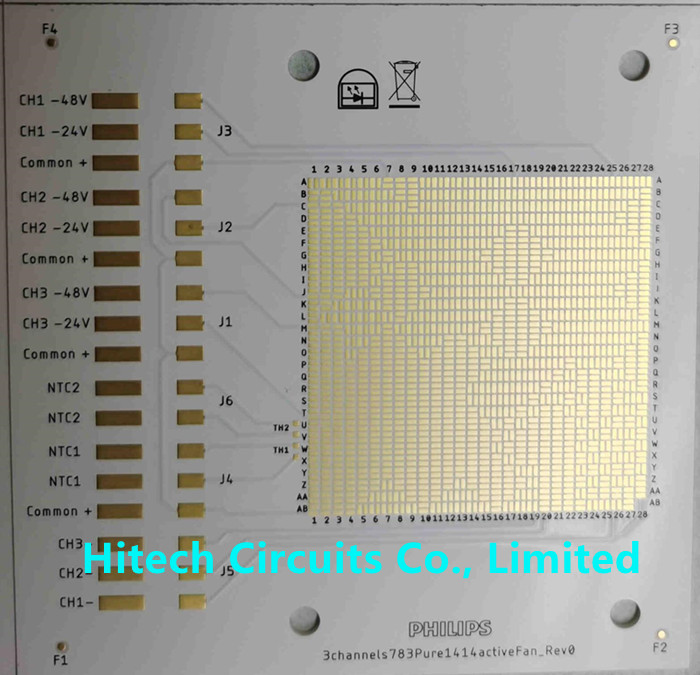
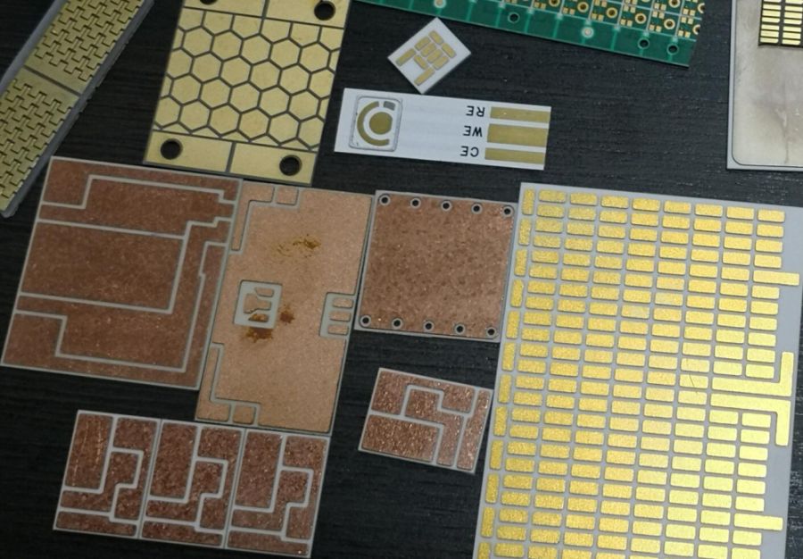
Ceramic PCB board is also called ceramic substrate or ceramic circuit board, ceramic copper coated plate, ceramic substrate refers to the copper foil directly bonded to alumina (Al2O3) or aluminum nitride (AlN) ceramic substrate or other ceramic substrate surface (single or double) on the special process board. The ultrathin composite substrate has excellent electrical insulation performance, high thermal conductivity, excellent soft brazing and high adhesion strength, and can be etched into a variety of graphics like PCB board, with great current-carrying capacity. Therefore, Ceramic PCB board has become the basic material of high power electronic circuit structure technology and interconnection technology.
Ceramic PCB Manufacturing & Assembly – One-stop service The ceramic substrate (ceramic PCB) refers to a special process board in which a copper foil is directly bonded to a surface of an alumina (Al2O3 ) or aluminum nitride (AlN) ceramic substrate (single or double-sided) at a high temperature. The ultra-thin composite substrate produced has excellent electrical insulation properties, high thermal conductivity, excellent solderability, and high adhesion strength, and can etch various patterns like a PCB board, and has a large current carrying current ability.
2. The advantages and disadvantages of Ceramic PCB
(1) Ceramic PCB board has very good thermal conductivity and insulation performance. Ceramic PCB board is made of ceramic substrate, ceramic substrate itself has very good insulation and thermal conductivity, thermal conductivity of 25~230w, insulation resistivity is 10 minus 14 square, visible insulation performance is very good.
(2) The dielectric constant of ceramic PCB board is very low, the dielectric loss is small, has very good high frequency performance, the dielectric loss of alumina ceramic PCB board is less than 0.0003@1MHz, the dielectric loss of aluminum nitride ceramic PCB board is less than 0.0005@1MHz. Low dielectric loss, high frequency performance, is widely used in the field of high frequency communication.
(3) Ceramic PCB bonding force is strong, using bonding technology, copper foil will not fall off.
(4) Ceramic PCB has large on-board flow, 100A current continuously passes through 1mm0.3mm thick copper body, and the temperature rises about 17℃; when 100A current continuously passes through the 2mm0.3mm thick copper body, the temperature rises only about 5℃.
(5) Ceramic PCB board is with high temperature resistance, corrosion resistance, environmental protection, can work in a very complex environment, long-term high frequency, long service life.
Disadvantages: fragile, scrap rate is high, this is one of the main short comings of ceramic PCB board, which leads to the production of a small area of the circuit board, the general size is less than 120mm, special custom 200mm,230mm, the general price is more expensive, the board cost is higher. In addition, because ceramic PCB board is made of ceramic material, it does not have better toughness like FR4 board, so it can make more than one meter long and wide. Another point is that the price is expensive, the requirements of electronic products are more and more rules, ceramic circuit boards are still used in some relatively high-end products, low-end products will not be used.
3. Number of Ceramic PCB production layers
Ceramic PCB board can do several layers at most, how many layers can be done, is a lot of customers more concerned about the topic. Ceramic PCB board can be made of multiple layers, mostly using HTCC process and LTCC process, but the processing cost is high. At present, Hitech circuit has made 4 layers, 8 layers, 16 layers of Ceramic PCB board, and so on, so far the customer feedback is good.
4. The introduction of Ceramic PCB board
Ordinary PCB is usually made of copper foil and substrate bonding, and the substrate is mostly glass fiber (FR-4), phenolic resin (FR-3) and other materials, adhesives are usually phenolic, epoxy, etc. In the process of PCB processing due to thermal stress, chemical factors, improper production technology and other reasons, or in the design process due to the two sides of the copper asymmetry, it is easy to lead to different degrees of PCB board warping.
And another PCB substrate - ceramic substrate, due to heat dissipation performance, current carrying capacity, insulation, thermal expansion coefficient, are much better than ordinary glass fiber PCB board, so it is widely used in high-power power electronic modules, medical electronics and other products.
Ceramic substrate and ordinary PCB using adhesive copper foil and substrate bonding together, Ceramic PCB is in the high temperature environment, through the bonding method of copper foil and ceramic substrate together, strong binding force, copper foil will not fall off, high reliability, stable performance in high temperature, high humidity environment.
5. Three materials of ceramic substrate
Al2O3
Al2O3 is the most commonly used substrate material in ceramic substrate because of its high strength and chemical stability compared to most other oxide ceramics in mechanical, thermal and electrical properties, and rich raw material sources, suitable for a variety of technical manufacturing and different shapes. According to the percentage of alumina (Al2O3) can be divided into: 75 porcelain, 96 porcelain, 99.5 porcelain. With different amounts of alumina, its electrical properties are almost unaffected, but its mechanical properties and thermal conductivity vary greatly. There is more glass in the substrate with low purity and the surface roughness is large. The higher the purity of the substrate, the cleaner, compact, the lower the dielectric loss, but the higher the price.
BeO
It has higher thermal conductivity than aluminum. It is applied to the occasions where high thermal conductivity is needed. It decreases rapidly after the temperature exceeds 300℃, but its toxicity limits its own development.
AlN
AlN are ceramics with aluminum nitride powder as the main crystalline phase. Compared with alumina ceramic substrate, the insulation resistance, insulation resistance and dielectric constant are higher. Its thermal conductivity is 7~10 times that of Al2O3, and its thermal expansion coefficient (CTE) is approximately matched with silicon wafer, which is very important for high-power semiconductor chips. In the production process, the thermal conductivity of AlN is greatly affected by the content of residual oxygen impurities, and the decrease of oxygen content can significantly improve the thermal conductivity. At present, it is no problem that the thermal conductivity of the production level reaches 170W/ (m·K).
For the above reasons, it can be known that alumina ceramics are in a leading position in the fields of microelectronics, power electronics, hybrid microelectronics and power modules due to their superior comprehensive performance. Compared with the same size on the market (100mm×100mm×1mm), different materials of ceramic substrate price: 96% alumina 9.5 yuan, 99% alumina 18 yuan, aluminum nitride 150 yuan, beryllium oxide 650 yuan, you can see that different substrate price gap is also relatively large.
Hitech Circuits is a professional and reliable manufacturer of Ceramic PCBs, with many years of experience in making Ceramic PCBs, which enables the manufacture of high technology, high quality and difficult performance boards, and guarantees the quality and reliability of every product delivered to customers. If you have the need to make Ceramic PCB, welcome to contact us!
6. Application of Ceramic PCB
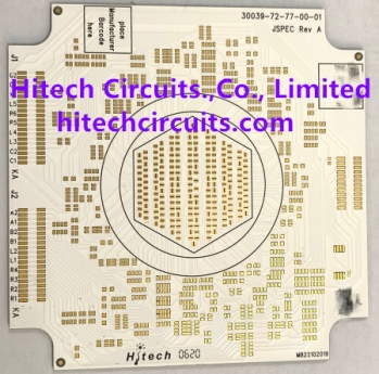
1. High power power electronics module, solar panel module, etc
2. High frequency switching power supply, solid state relay
3. Automotive electronics, medical electronics
4. High power LED lighting products
5. Communication antenna, automobile igniter
7. Why use Ceramic PCB instead of other PCB boards?
Ordinary PCB is usually made of copper foil and substrate bonding, and the substrate is mostly glass fiber (FR-4), phenolic resin (FR-3) and other materials, adhesives are usually phenolic, epoxy, etc. The main material of ceramic substrate is alumina (Al2O3), beryllium oxide (BeO), aluminum nitride (AlN) and other metal oxide ceramics, the performance of the two is quite different.
● Plate rigidity, ordinary PCB basically belongs to chemical fiber material, its environment, temperature, processing technology and other conditions, its rigidity is far less than ceramic substrate; The latter has strong thermal stability and small coefficient of thermal expansion, which can be used in harsher environments.
● Heat dissipation performance, ceramic substrate heat dissipation performance is excellent, very suitable for high-power device scenarios, and ordinary PCB is currently limited by material technology, far less than ceramic materials.
● Insulation performance, good insulation of ceramic substrate, high pressure resistance, effectively protect personal safety and equipment.
● The bonding force between ceramic substrate and copper foil is strong, the bonding technology is used, the copper foil will not fall off, which greatly improves the reliability of the plate
8. What are the characteristics of Ceramic PCB
● Good stability
The surface of this plate can play a very good flame retardant effect, and good fire resistance, not easy to melt, Ceramic PCB is all acid and alkali items and other chemicals, whether it is disinfectant or cleaning agent, the surface of the Ceramic PCB will not be affected.
● Easy to clean
The surface of the Ceramic PCB has a strong anti-corrosion function, so it is very convenient to clean, the use of washing solution cleaning will not cause any impact on the surface and color, and the surface is very tight, no penetration, not easy to adhere to dust, but also has moisture-proof performance.
● Beautiful
The plate before firing, can be painted on the surface of the pattern and pattern, so fired out of the Ceramic PCB picture color is very beautiful, and not easy to be damaged, such Ceramic PCB is very beautiful and generous, and most are used for decoration.
● Anti-static
Ceramic PCBs are antistatic materials.
● Resistance to scratch
The surface structure of this kind of plate is very special, even under the action of hard objects outside, it is not easy to cause damage.
9. Ceramic PCB Classification
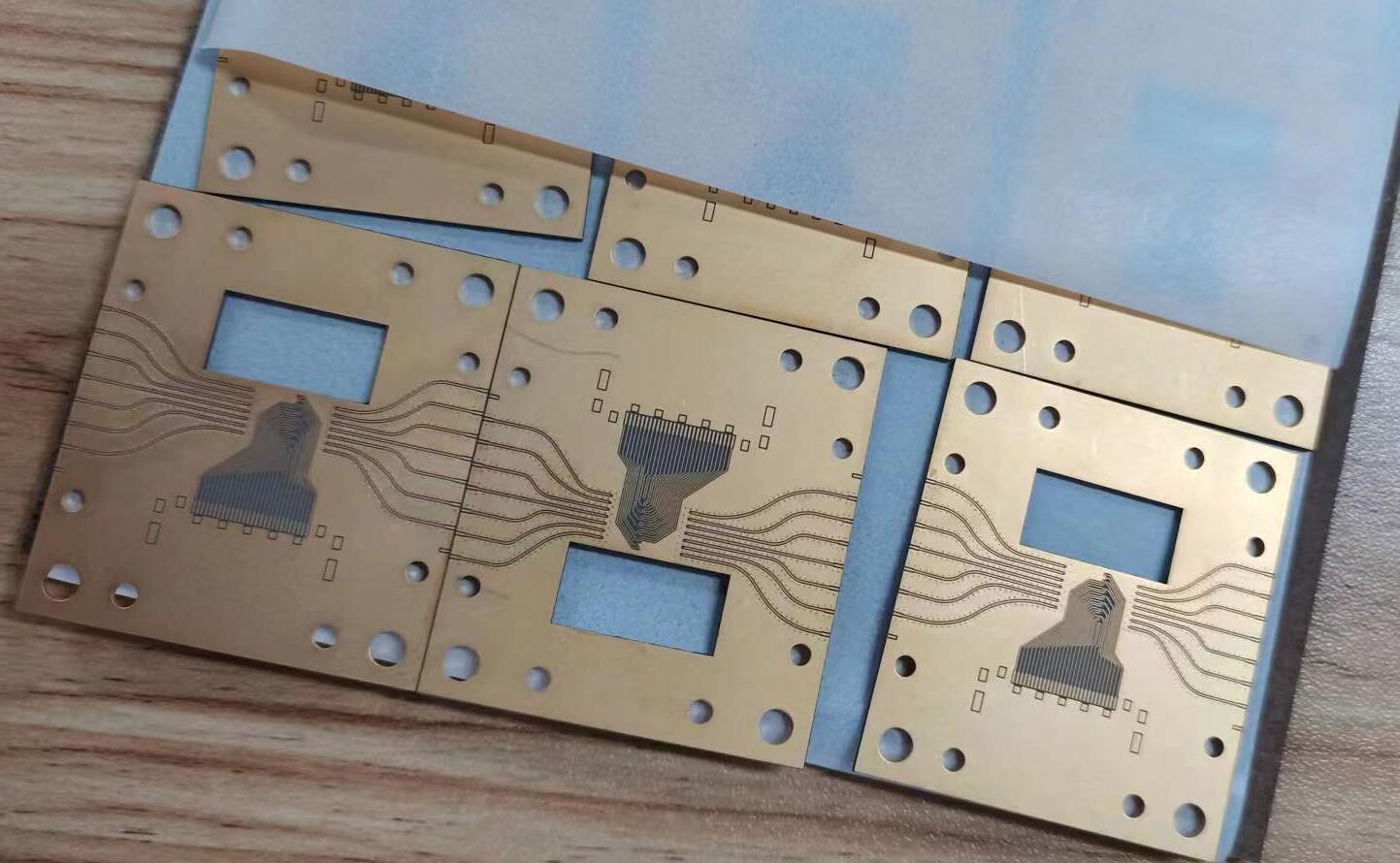
1. According to the material Alumina (Al2O3) Ceramic PCB Beryllium Oxide (BeO) Ceramic PCB Aluminum Nitride (ALN) Ceramic PCB
2. According to the manufacturing process HTCC (High-Temperature Co-fired Ceramic) LTCC (Low-Temperature Co-fired Ceramic) DBC (Direct Bonded Copper) DPC (Direct Plate Copper) Ceramic PCB is a thermal conductive organic ceramic circuit board with high thermal conductivity and prepared at a temperature below 250°C using thermally conductive ceramic powder and organic adhesive, ceramic PCB types by material including alumina pcb, Aluminum nitride ceramic PCB, Copper clad ceramic PCB, Zirconia ceramic base PCB.
10. Four types: HTCC, LTCC, DBC, and DPC
1. The HTCC (high temperature co-fired) preparation method requires a temperature above 1300°C, but due to the choice of the electrode, the preparation cost is quite expensive.
2. The LTCC (low temperature co-firing) requires a calcination process of about 850°C, but circuit precision is poor, and the thermal conductivity is low.
3. The DBC requires formingan alloy between the copper foil and the ceramic, and the calcination temperature needs to be strictly controlled within the temperature range of 1065-1085°C. Because the DBC requires the thickness of the copper foil, generally, it cannot be less than 150-300 microns. Therefore, the wire width to depth ratio of such ceramic circuit boards is limited.
4. The preparation methods of DPC include vacuum coating, wet coating, exposure and development, etching, and other process links, so the price of its products is relatively high. In addition, in terms of shape processing, DPC 1800 ceramic fiber board plates need to be laser cut. Traditional drilling and milling machines and punching machines cannot accurately process them, so the bonding force and line width are more precise.
11. Ceramic PCB HTCC and LTCC process
HTCC full name of High Temperature co-fired Ceramic, called multi-layer high temperature co-firing technology. Usually used for multilayer ceramic circuit boards, and then high precision, high integrated circuit applications.
LTCC full name of Low Temperature co-fired Ceramic, known as low temperature co-fired ceramic technology. LTCC technology involves layering ceramic materials as required, printing interconnecting conductors, components and circuits internally, and firing them into an integrated ceramic multilayer material.
HTCC and LTCC process material difference
The high-temperature co-fired ceramics of HTCC are mainly composed of alumina, mullite and aluminum nitride, and the ceramic powder of HTCC does not include glass material. Due to the high firing temperature of HTCC substrate, low melting point metal materials such as gold, silver and copper cannot be used, while conductor paste materials are tungsten, molybdenum, molybdenum, manganese and other high melting point metal heating resistance paste.
LTCC low-temperature co-fired ceramics in order to ensure high sintering density under low-temperature co-fired conditions, amorphous glass, crystallized glass, low melting point oxides, etc. are usually added to the components to promote sintering. Glass and ceramic composite is a typical low temperature co-fired ceramic material. In addition, there are crystallized glass, crystallized glass and ceramic composites and liquid phase sintered ceramics. The metals used are high conductivity materials (Ag, Cu, Au and their alloys, such as Ag-Pd, Ag-Pt, Au-Pt, etc.), which can not only reduce the cost, but also obtain good performance.
HTCC and LTCC process differences
The overall technological process of LTCC and HTCC is very similar. Both of them have to go through the preparation process of slurry preparation, casting strip, drying green blank, drilling through hole, screen printing hole filling, screen printing line, laminated sintering, and finally slicing. The equipment required is similar. However, due to the big difference in materials, the co-firing temperature of LTCC and HTCC in the production process is quite different. HTCC has a sintering temperature above 1650℃, while LTCC has a sintering temperature below 950℃. The LTCC process has been developed due to the high sintering temperature, huge energy consumption and limited metal conductor materials of HTCC substrate.
HTCC and LTCC application differences
● LTCC application of Ceramic PCB
LTCC uses Au, Ag, Cu and other metals with high conductivity and low melting point as conductor materials. Due to the low dielectric constant and high frequency and low loss properties of glass ceramics, LTCC is very suitable for application in radio frequency, microwave and millimeter wave devices. It is mainly used in the field of high frequency wireless communication, aerospace, memory, drivers, filters, sensors and automotive electronics.
Commonly used LTCC electronic components include filters, diplexers, antennas, barron, couplers, power splitters, common mode chokes, etc., widely used in mobile communication terminals, WiFi, automotive electronics, T/R components and other fields.
● Application of HTCC of Ceramic PCB
Due to high sintering temperature, HTCC cannot use gold, silver, copper and other low melting point metal materials, must use tungsten, molybdenum, manganese and other refractory metal materials, these materials have low electrical conductivity, will cause signal delay and other defects, so it is not suitable for high-speed or high-frequency microassembled circuit substrate. However, because HTCC substrate has the advantages of high structural strength, high thermal conductivity, good chemical stability and high wiring density, it has a wide application prospect in high-power microassembled circuits. Because of its high thermal conductivity, good structural strength and stable physical and chemical properties, HTCC ceramic substrate is widely used in high reliability microelectronics integrated circuits, high-power microassembly circuits, high-power on-board circuits and other fields.
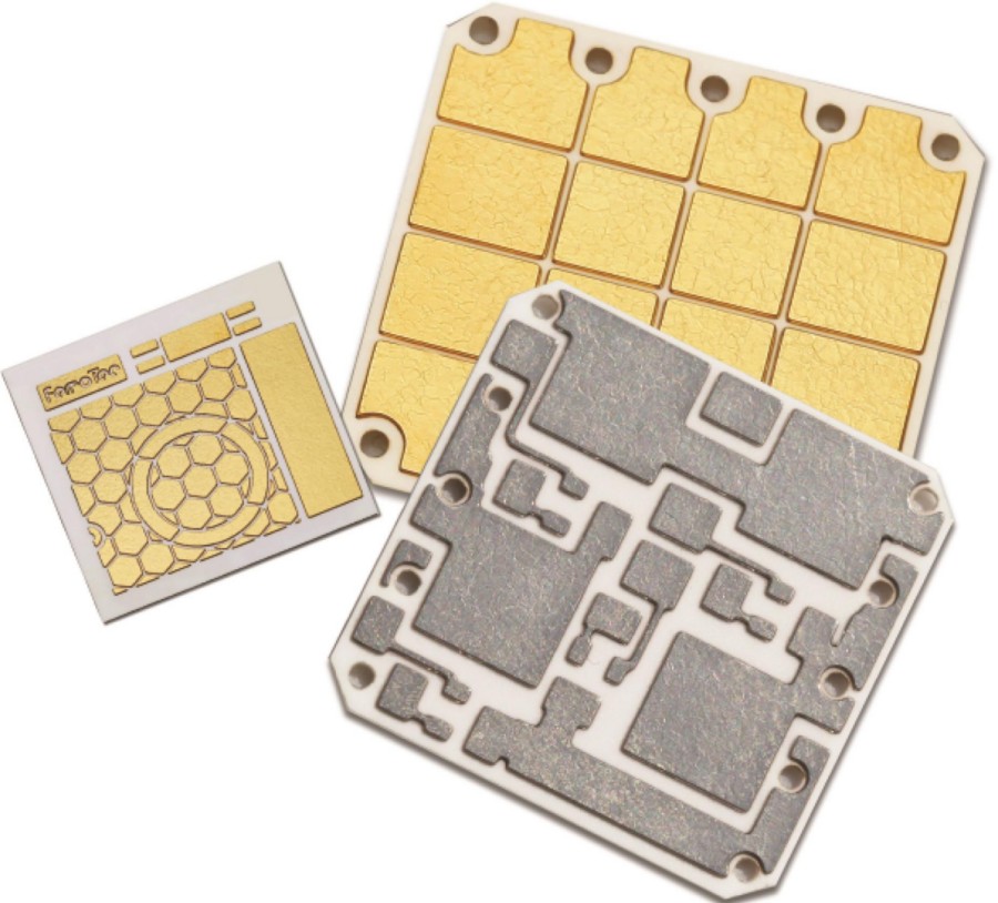
12. Why Ceramic PCB has such excellent performance?
96% or 98% Alumina (Al2O3), Aluminum Nitride (ALN), or Beryllium Oxide (BeO)
Conductors material: For thin film technology, thick film technology, it’ll be silver palladium (AgPd), gold pllladium (AuPd); For DCB (Direct Copper Bonded) it’ll be copper only
Application temp: -55~850℃
Thermal conductivity value: 16W~28W/m-K (Al2O3); 150W~240W/m-K for ALN , 220~250W/m-K for BeO;
Max compression strength: >7,000 N/cm2
Breakdown Voltage (KV/mm): 15/20/28 for 0.25mm/0.63mm/1.0mm respectively
Thermal expansion conefficient(ppm/K): 7.4 (under 50~200℃)
13. Why Purchase Your Ceramic PCBs from Hitechpcb?
At HITECH CIRCUITS, we are dedicated to producing and selling quality PCBs to all of our customers. With over 15 years of experience in the electronic industry we are committed to producing custom ceramic PCBs that meet up with the various electronic devices at hand. Our professionals manufacture nothing but top-notch ceramic PCBs that are developed to tackle your demands. In addition, we assure that you will get nothing but the best and affordable prices for all the quality ceramic PCB we manufacture. Regardless of the quality of the printed circuit boards that you want, it will be gotten at a decent price.

0086-755-29970700
sales@hitechpcb.com; sales@hitechcircuits.com
2F, Building C, Suojia Technology Park, Hangcheng, Bao’an, Shenzhen, Guangdong, China 518126
 Chinese
 English
 Russian
 Spanish
 Portuguese


