 Chinese
 English
 Russian
 Spanish
 Portuguese
High Frequency PCB Design
Excellent Quality
- 100+ PCB Design & Layout projects per year
- Outstanding designers with 10+ working experiences.
- 7/24 Live sales & tech support
- 6 hours PCB Layout expedite services
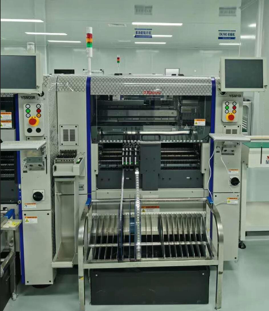
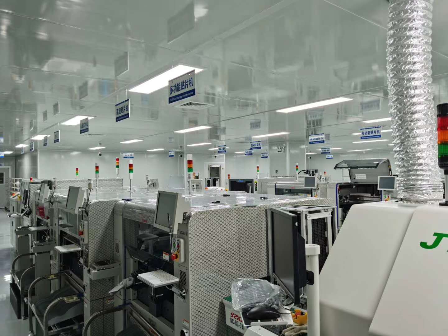
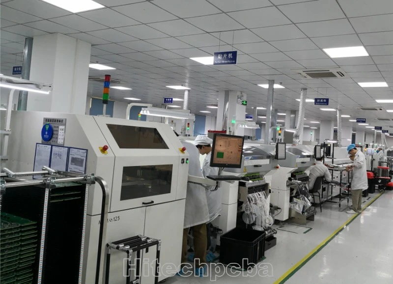
Company Show

Advantages Of Our PCB Design
- Min.trace width 2.5mil,
- Min trace spacing 2.5mil,
- Min vias 6mil ( 4mil laser drilling),
- Max layer count 38 layers,
- Min BGA spacing 0.4mm,
- Max BGA Pin 2500pin,
- HDI highest Layer count 18 layers,
- Fastest delivery time 6 hours per item.
High Frequency PCB Design
What is High frequency PCB?
High frequency PCB refers to high frequency circuit board. At present, high frequency and induction heating technology has the highest heating efficiency, the fastest speed, low consumption and environmental protection. It has been widely used in hot processing, heat treatment, hot assembly, welding, smelting and other processes of metal materials in all walks of life. It can not only heat the workpiece as a whole, but also heat the workpiece locally; It can realize the deep heat penetration of the workpiece, or only the surface and surface can be heated centrally; It can not only directly heat metal materials, but also indirectly heat non-metallic materials. Therefore, induction heating technology will be more and more widely used in all walks of life.
High Frequency PCB or calls Radio Frequency PCB/RF PCB are widely used in wireless communications, wireless networks and satellite communications, in particular the popularity of 3G networks exacerbate the market demand for the product on the High Frequency PCB. Today, the demand for Microwave material PCB design is on the rise, Access to wireless high speed (high frequency) data is quickly becoming a necessity in multiple markets like Defense、Aerospace and Mobile Networks. Evolving market needs continue to drive forward development of High Frequency printed circuit board. like 50+ GHz microwave radios or defense airborne systems, also it can meet Halogen Free PCB together.

RF PCB & High-Frequency PCB made from polytetrafluoroethylene (PTFE PCB), ceramic filled fluoropolymer, or ceramic filled hydrocarbon thermosets materials with improved dielectric properties. this material have a low dielectric constant of 2.0-3.8, a low loss factor and excellent low loss characteristics, also with favorable properties are high glass transition temperature, a very low hydrophilic rate, an excellent thermal durability. The expansion coefficient of PTFE PCB material is similar to the copper which allows the material to exhibit excellent dimensional stability.
HitechPCB company has increased the investment of production equipment and research & development on High Frequency PCB field over the last few years, It is to meet to market development of the RF PCB for our customers from all around the world, We have rich experience in PTFE PCB manufacturing of various high-frequency circuit boards for quick turn prototypes and mass production. Our normal Teflon material supplier including: Rogers PCB, Nelco PCB,Taconic PCB, Arlon PCB, etc.
Features of High Frequency PCB Boards
1.These typically have a low dielectric constant (approximately 2.40) and have tight tolerances.
2. They feature a small dissipation factor. Hence, they have a low loss tangent. Therefore, it allows for faster signal propagation and low signal distortion. So, they are suited for high frequency applications that demand high reliability.
3. These have a thermally stable structure because they have a relatively low Z-axis CTE. So, the low CAF resistance and the low Z-CTE leads to a long lifespan for these PCBs.
4. They feature excellent dimensional stability. Hence, ideal for applications involving extreme environmental conditions.
5. These feature small moisture absorption. Hence, they provide excellent resistance against heat and moisture.
6. They have ideal properties for reflow conditions. Hence, they are favorable for industrial application.
Introduction for High Frequency PCB design
In high frequency PCB design, the power supply is designed as a layer, in most cases much better than a bus, so that the circuit can always follow the path with the least impedance. In addition, the power board must provide a signal circuit for all generated and received signals on the PCB, which minimizes the signal circuit and thus reduces noise. This point is often overlooked by low-frequency circuit designers.

1
Composition of high frequency PCB:
-Solder side: metal hole for welding components.
-Via hole: there are two types of metal via hole and non-metal. Metal is used mainly to connect the components of the layers.
-Installation hole: used for fixed circuit board.
-Conductor trace line: electrical network copper film used to connect the components of the components.
-Connector: the components that are used between the circuit boards.
-Fill: copper applied to the ground line network can effectively reduce the impedance.
-Electrical boundary: to determine the size of the circuit board, all the components on the board cannot exceed the boundary.
2
Components layout
When making high frequency PCB board, the designer should first consider the electrical performance between components. Only when the electrical properties of the PCB meet the requirements can the designer consider the convenience of wiring and other properties of the PCB.
a, The electrical property
In the layout, the designer should make the components to close electrical relationship as close as possible, especially for the wiring between some components with high frequency. Because the connection between these components is relatively short. For high-power devices, the layout should be separated from some small signal devices to reduce the interference to small signal devices. Then, if the system is composed of multiple PCB boards, high-speed devices with these characteristics should be placed on the same PCB board as far as possible. It avoids the problem of shift errors to cause the unequal clock signal transmission delay time between the main PCB board and different plug-in boards.
For example: In the layout of high-speed Ethernet, the anti-interference resistance capacitance of Ethernet chip DM9000 and PH163539 should be attached around the core chip as far as possible.
Electronic property
b, Routing
Basic principles of routing:
- Unified and stable between power supply and ground.
- Carefully considered routing and proper terminations can eliminate reflections.
- Carefully considered routing and proper terminations can reduce capacitive and inductive crosstalk.
- Suppress noise to meet EMC requirements.
c, Ground wire and Volt current condenser
If the ground wire or power supply layout on a high frequency PCB is not reasonable, the PCB will produce electromagnetic interference. It means that the high frequency PCB performance will be degradation. Worse still, the PCB might just stop working.
There is an equation for gap capacitance between ground and power supply:
Equation
Xc-Capacitance reactance, ω-Pin frequency, f-signal frequency, C-capacitance(farad)
It can be seen from the equation, the greater the gap capacitance between the ground and the power supply, the less its capacitance resistance will be, and at the same time, it will produce noise interference.
Methods to reduce noise between ground and power supply:
(1) Increase line width and reduce noise.
(2) Common ground processing to reduce modulus interference.
(3) Conduct signal wire wiring on the power supply or ground wire layer.
d, Material requirements
1. Dissipation factor (Df) must be small (and stable)
2. Dielectric constant (DK) must be small (and stable)
3. Low water absorption
4. The thermal expansion coefficient of copper foil should be as close as possible
5. Heat resistance, chemical resistance, impact strength and peel strength shall be maintained in good condition.
3
High frequency PCB manufacturing notes
a, Impedance control requirements and relative line width control are relatively strict. Their tolerance is generally around 2%.
b, As the special plate, PTH does not have a high adhesion. It is usually necessary to roughen the pores and surface with the help of plasma treatment equipment. This is to increase the adhesion of PTH copper hole and solder ink.
c, It cannot grind the plate until it has been blocked. This is because it will reduce the adhesion, so that it can only be used with a micro etching potion for coarsening.
d, Most of boards is Teflon PCB type of materials. Therefore, this requires the use of special milling cutters, if the producer uses ordinary milling cutters, there are many rough edges on the board.

Manufacturing requirements of high frequency board
High frequency PCB board is one of the most difficult boards, so it must meet the manufacturing requirements as much as possible.
Drilling
1. The drilling feed speed should be slow, 180 / s. A new drill nozzle should be used, and aluminum sheets should be placed on the top and bottom. It is best to drill with a single PNL, and no water can be encountered in the hole
2. Concentrated sulfuric acid (preferably not used) can be used for PTH pore template of pore finishing agent for 30min
3. The grinding plate copper sinking line is made as normal double-sided
4. Special attention: the high-frequency board does not need to remove the glue residue.
Anti welding
1. If the high-frequency plate needs green oil backing, it is not allowed to grind the plate before resistance welding, and a red seal shall be stamped in MI.
2. If the high-frequency board needs to be printed with green oil on the substrate, it shall be printed with green oil twice (to prevent green oil foaming on the substrate). The Board shall not be ground before etching and tin withdrawal, but can only be air dried. For the first time, the 43T screen plate shall be used for normal printing of segmented baking plate: 50 ° 50min, 75 ° 50min, 95 ° 50min, 120 ° 50min, 135 ° 50min, 150 50min. The plate shall be exposed with line film, grinded after development, and made normally for the second time. Note in MI: line film alignment is used for the first priming.
3. If the high-frequency board needs to be printed with green oil on some substrates and not on some substrates, it needs to produce a "backing film". The backing film only retains the green oil on the substrate, and the second normal production can be carried out after the backing baking board. The following picture shows the need of 018212, especially the "backing film".
Special attention should be paid to printing green oil only once if it is not printed on the substrate like 018092 (see the figure below, the blue part is the green oil window), so as to prevent the green oil on the substrate from developing after the first green oil priming.
Tin spraying
Before tin spraying, bake 150 degrees for 30 minutes before tin spraying
Line tolerance
The line width tolerance without requirements shall be ± 0.05mm. If required, it shall be made according to the customer's requirements.
Plate
To use the specified plate, see requirements. Because the plate price is expensive, only 1pnl can be opened.
High frequency PCB material selection
In recent years, the continuous introduction of wireless communication, optical fiber communication and high-speed data network products, high-speed information processing and wireless analog front-end modularization have put forward new requirements for digital signal processing technology, IC process and Microwave PCB design, as well as higher requirements for PCB plate and PCB process. For example, commercial wireless communication requires the use of low-cost plates and stable dielectric constant( ε R variation error is between ± 1-2%), low dielectric loss (below 0.005). Specific to the PCB board of mobile phone, it also needs to have the characteristics of multi-layer lamination, simple PCB processing technology, high reliability of finished board, small volume, high integration and low cost. In order to challenge the increasingly fierce market competition, electronic engineers must make a compromise between material performance, cost, difficulty of processing technology and reliability of finished boards. At present, there are many plates available for selection, and the representative commonly used plates are: epoxy resin glass cloth laminate FR4, polyester fluoroethylene PTFE, polytetrafluoroethylene glass cloth F4, modified epoxy resin FR4, etc. Special plates, such as sapphire substrate and ceramic substrate used in satellite microwave transceiver circuit; Microwave circuit substrate GX series, ro3000 series, ro4000 series, TL series, TP-1 / 2 series, f4b-1 / 2 series. They are used on different occasions, such as FR4 for mixed signal circuits below 1GHz, polyvinylidene fluoride PTFE for multi-layer high-frequency circuit boards, Teflon glass cloth fiber F4 for double-sided microwave circuit boards, and modified epoxy resin FR4 for high-frequency heads of household appliances (below 500MHz). FR4 plate is widely used because of its easy processing, low cost and easy lamination. Next, we analyze the characteristi
PCB manufacturers, PCB designers and PCBA manufacturers explain how to design high-frequency PCB boards for microwave circuits
This paper focuses on the concept and planning principles of microwave grade high frequency circuit/microwave circuitcs of microstrip transmission line, multilayer plate lamination process, plate parameter performance comparison and other aspects, give the selection scheme of PCB plate for special applications, and summarize the key points of high-frequency signal PCB design for the reference of electronic engineers.
How to design high frequency pcb board of microwave circuit
High frequency PCB board, which is a frontier field of communication products. The reason why microwave grade high frequency circuit/ high frequency PCB board planning principle of microwave circuit is selected is that this principle has extensive guiding significance and is a popular high-tech application technology at that time. The transition from microwave circuit high frequency pcb board planning concept to high-speed wireless network (including various access networks) project is also consistent, because they are based on the same fundamental principle - dual transmission line theory.
Experienced high-frequency microwave and RF engineers plan digital circuits or high-frequency PCB boards with relatively low frequency circuits. The one-time success rate is very high, because their planning concept is centered on "distributed" parameters, and the destructive effect of the concept of distributed parameters in lower frequency circuits (including digital circuits) is often ignored.
High-frequency PCB board planning principles involve many aspects, including the basic principles, anti-interference, electromagnetic compatibility, security protection, and so on. With regard to these aspects, the lack of relevant concepts, especially in high-frequency circuits/microwave circuits (especially in microwave grade high-frequency circuits), often leads to the failure of the entire R&D project. Many people still stay on the basis of "connecting electrical principles with conductors to play a predetermined role", and even think that "the planning of high-frequency pcb boards belongs to the consideration field of structure, process and improving production power". Many professional high-frequency microwave and RF engineers have not fully realized that this link should be the key to the entire high-frequency pcb board planning in RF planning, and they mistakenly spent their energy on selecting high function components, resulting in a substantial increase in cost, but little progress in function.
In particular, it should be pointed out that digital circuits rely on their strong anti-interference, error detection and correction, and arbitrary structure of each intelligent link to ensure the normal function of the circuit. A general figure uses circuits to configure various "ensure normal" links with high addition, which obviously belongs to the action without product concept. However, the link that is often considered "unworthy" leads to a series of product problems. The reason is that such functional links, which are not worth ensuring structural reliability from the perspective of product engineering, should be based on the operation mechanism of the digital circuit itself, but only on the error structure in circuit planning (including high-frequency pcb board planning), resulting in an unstable circuit. As a result of this instability, similar problems with high-frequency circuits/microwave circuits belong to the fundamental application of the same concept.
In digital circuits, there are three aspects that deserve serious attention:
All kinds of reliability planning in the application of digital circuits are related to the reliability requirements of circuits in practical application and product engineering requirements. It is not allowed to add various high cost "guarantee" parts to circuits that can fully meet the requirements with conventional planning.
2. The operation rate of digital circuits is moving towards high frequency with unprecedented development (for example, the main frequency of current CPUs has reached 1.7GHz, far exceeding the lower limit of microwave frequency band). Although the reliability assurance functions of related devices are also synchronized, they are based on the internal and typical external signal characteristics of devices.
3. Digital signals themselves belong to broad-spectrum signals. According to the results of Fourier function, it contains rich high-frequency components, so the high-frequency weight of digital signals is fully considered in the planning of digital ICs. However, in addition to digital ICs, signal transition areas within and between functional links will lead to a series of problems if they are carried out arbitrarily. Especially in the digital and analog and high-frequency circuit (high-frequency pcb board) mixed use of the circuit occasions. PCB manufacturers, PCB designers and PCBA manufacturers will explain how to design high-frequency pcb boards for microwave circuits.

High frequency circuit design is a very complex design process, and its wiring is very important to the whole design! Next, I would like to share some wiring skills of high frequency PCB design. High frequency PCB wiring skills
1. Multilayer board wiring high-frequency circuit is often high integration, wiring density, using multilayer board is not only necessary for wiring, but also an effective means to reduce interference. In the PCB layout stage, reasonable selection of PCB size with a certain number of layers can make full use of the intermediate layer to set the shielding, better realize the nearby grounding, effectively reduce the parasitic inductance and shorten the transmission length of the signal, at the same time, greatly reduce the cross interference of the signal, etc. all these methods are beneficial to the reliability of high-frequency circuit.
2. The shorter the lead, the better the radiation intensity of the signal is proportional to the length of the signal line. The longer the high-frequency signal lead is, the easier it will be coupled to the components close to it. Therefore, for high-frequency signal lines such as signal clock, crystal oscillator, DDR data, LVDS cable, USB cable, HDMI line, etc., the shorter the wiring is, the better.
3. The less the lead is bent, the better. The lead wire of high frequency circuit is best to adopt full straight line, which can be turned by 45 degree broken line or arc. This requirement is only used to improve the fixation strength of copper foil in low-frequency circuit, but in high-frequency circuit, meeting this requirement can reduce the external emission and coupling of high-frequency signals.
4. The less interlaminar alternation, the better. The so-called "less interlaminar alternation of leads, the better" means that the less vias (via) used in the process of component connection, the better. It is measured that a via can bring about 0.5pf distributed capacitance. Reducing the number of vias can significantly improve the speed and reduce the possibility of data error.
5. Pay attention to the "crosstalk" caused by the close parallel routing of signal lines, and the crosstalk refers to the coupling phenomenon between signal lines that are not directly connected. Because the high frequency signal is transmitted in the form of electromagnetic wave along the transmission line, the signal line will act as an antenna, and the energy of electromagnetic field will be transmitted around the transmission line. The unwanted noise signal generated by the mutual coupling of electromagnetic fields between signals is called crosstalk. The parameters of PCB layer, the spacing of signal lines, the electrical characteristics of driver and receiver, and the termination mode of signal line have certain influence on crosstalk.
6. Add a high frequency decoupling capacitor to the power pin of the IC block, and add a high frequency decoupling capacitor to the power pin of each IC block. Increasing the high-frequency decoupling capacitance of the power supply pin can effectively suppress the high-frequency harmonic interference on the power supply pin.
7. The ground wire of high-frequency digital signal is isolated from the ground wire of analog signal. When the analog ground wire and digital ground wire are connected to the common ground wire, they should be connected with high-frequency choke magnetic beads or directly isolated, and the appropriate single point interconnection should be selected. The ground potential of the ground wire of high frequency digital signal is generally inconsistent, and there is a certain voltage difference between them. Moreover, the ground wire of high-frequency digital signal often has a very rich harmonic component of high-frequency signal. When the ground wire of digital signal is directly connected with the ground wire of analog signal, the harmonic of high-frequency signal will interfere with the analog signal through the coupling of ground wire. Therefore, in general, the ground wire of high-frequency digital signal and the ground wire of analog signal should be isolated. Single point interconnection at appropriate position or high-frequency choke magnetic bead interconnection can be used.
8. Avoid the loop formed by wiring. Try not to form a loop for all kinds of high-frequency signal wiring. If it is unavoidable, make the loop area as small as possible.
9. Good signal impedance matching must be ensured. In the process of transmission, when the impedance does not match, the signal will reflect in the transmission channel, which will cause the synthetic signal to form overshoot and cause the signal to fluctuate near the logic threshold. The fundamental way to eliminate the reflection is to make the impedance of the transmission signal match well. Since the greater the difference between the load impedance and the characteristic impedance of the transmission line, the greater the reflection will be. Therefore, the characteristic impedance of the signal transmission line should be equal to the load impedance as far as possible. At the same time, it should be noted that the transmission line on the PCB should not have abrupt changes or corners, and try to keep the impedance of each point of the transmission line continuous, otherwise there will be reflection between each section of the transmission line.
10. Keep the integrity of signal transmission, keep the integrity of signal transmission, and prevent "ground bounce" caused by ground wire division.
Why do you need to focus on choosing the right manufacturer?
Ordering PCB manufacturing from a high tech equipped facility can be more beneficial than getting it manufactured in a low-cost manufacturing facility with low-grade material used.
RF PCBs are highly sensitive towards factors such as noise, impedance, electromagnetism, and esds. High-quality PCB manufacturers focus on eliminating any affecting factors during manufacturing. A poor quality RF Microwave PCB is not expected to sustain for long, and that’s why choosing a perfect RF PCB manufacturer can alter your product experience.
Today, most of the modern RF PCB manufacturing facilities use Computer Aided Engineering software simulation programs for PCB manufacturing. The best advantage of CAD-based RF Microwave PCB manufacturing is that it has simulation models of various brands and PCB models with proper product specifications.
These parameters are essential in the production of a standardized RF Microwave PCB and ensure reliability. Furthermore, the machines also support manual functioning, allowing the operator to perform manual operations.
So, it is evident that RF Microwave PCB manufacturing is not as simple as it seems.
Why choose HITECH CIRCUITS for your High Frequency PCB, RF Microwave PCB manufacturing?
RF PCB Manufacturer
HITECH CIRCUITS has specialized in Rogers PCB materials and prefers it for RF Microwave PCB manufacturing. The diverse range of Rogers PCB materials allows us to choose the most suitable material according to requirements.
HITECH CIRCUITS has been dealing in RF PCB manufacturing facilities for diverse products all over the globe. The qualified professionals at HITECH CIRCUITS have expertise in Rogers PCB manufacturing. Fortunately, HITECH CIRCUITS has experienced RF Microwave PCB manufacturing for M communication equipment.
The material used in m equipment for PCB assembly was Rogers 4003c, Rogers 4350 and RT5880. This SMT based dual layer assembly incorporated 350 deployments. The final product was tested at an automated x-ray and optical equipment. The quality assurance department thoroughly examined each product. The products were delivered after complete satisfaction of multiple departments.
Since HITECH CIRCUITS has been into PCB product development and with a diverse experience of assisting project developers from various fields, HITECH CIRCUITS has developed a long-lasting relationship with its satisfied clients.
One of the primary reasons why you should consider HITECH CIRCUITS is its technical support always available just a few clicks away. HITECH CIRCUITS technical team is always available for technical support. If you are looking for a manufacturing company that will help you through out your RF PCB manufacturing process and will share ideas and strategies for your product development, you should consider HITECH CIRCUITS
Benefits of getting your RF PCB manufactured by HITECH CIRCUITS
RF Microwave PCBs are not easy to manufacture unlike regular PCBs and requires detailed monitoring of various factors, being an experienced RF Microwave PCB manufacturer, HITECH CIRCUITS has developed the experience of handling RF projects and knows precisely how to incorporate these factors. HITECH CIRCUITS is a renowned PCB manufacturing brand all over the globe. The quality products and satisfactory experience of our clients uplift our image.
Trusting a PCB manufacturer with your sensitive product can be difficult, and we truly understand that. HITECH CIRCUITS not only assists its clients during the manufacturing process but offers detailed technical support even after the manufacturing of PCB.
We ensure that your PCB manufacturing is not just developed but the product functions exactly as required and before manufacturing, the technical experts at HITECH CIRCUITS analyze the complete design for any possible flaws or cushion for improvements. Accordingly, customer concerns are considered, and a reliable product is developed.
If, a design lacks over any specifications or required featuring, our team is liable to discuss with the customer and offer alternatives. Furthermore, the client is saved from the hustle of testing as our testing team performs various tests at your custom RF Microwave PCB and makes sure that it serves the purpose.

0086-755-29970700
sales@hitechpcb.com; sales@hitechcircuits.com
2F, Building C, Suojia Technology Park, Hangcheng, Bao’an, Shenzhen, Guangdong, China 518126


