 Chinese
 English
 Russian
 Spanish
 Portuguese
Flexible PCB Manufacturing
Flexible PCB Manufacturing
What is Flex PCB?
Flexible printed circuits, also known as flex circuits, are sometimes regarded as a printed circuit board (PCB) that can bend, when in reality there are significant differences between PCB’s and flex circuits when it comes to design, fabrication and functionality. One common mistake that designers make is to design a flexible circuit using the same rules as a PCB. Flex PCB require a unique set-up and have their own set of design rules that the Hitechpcb team has termed “flex-izing” and have worked hard to perfect over the last many years.
Flexible PCB, which also called Flex PCB, Flexible circuit board or flex circuit, it consists of PI base material, adhesive layer, copper layer, coverlay and sometimes with stiffeners. Flexible PCBs are now being used widely to replace traditional FR4 PCB in various different applications due to the benefits from flex PCB specially. Although more expensive than a normal rigid PCB, the right design in the right application could save weight and time in assembly, coupled with the reliability which makes flexible circuit board a worthwhile consideration.
A flexible printed circuit consists of a metallic layer of traces, usually copper, bonded to a dielectric layer, usually polyimide. Thickness of the metal layer can be very thin (<.0001″) to very thick (> .010″) and the dielectric thickness can vary from .0005″ to .010″. Often an adhesive is used to bond the metal to the substrate, but other types of bonding such as vapor deposition can be used to attach the metal.

How to calculate your flex pcb bend radius?
Because copper tends to readily oxidize, the exposed surfaces are often covered with a protective layer, gold or solder are the two most common materials because of their conductivity and environmental durability. For non-contact areas a dielectric material is used to protect the circuitry from oxidation or electrical shorting.
The number of material combinations that could go into a flexible printed circuit are nearly endless; current, capacitance, chemical and mechanical resistance, temperature extremes and type of flexing are just some of the criteria that impacts the material selections that best meet the functional needs. An experienced Hitechpcb design engineer takes the critical requirements into consideration when designing a circuit to meet your needs.
Flexible printed circuit boards (FPC) has become a common component of electronic products due to its lightness and flexibility performance. It is widely used in smart terminal, wearable electronics, consumer, automotive, industrial and medical fields. The miniaturization and integrated function of electronics product development is driving FPC to fine line and multilayer design.
What is Multilayer flex PCB?
This type of flexible printed wiring boards are multilayered (with three or more conductor layers) and require plated-through holes. We could use through vias, buried vias and blind vias.
A multi layer flex circuit combine several single-sided or double-sided circuits with complex interconnections, shielding and/or surface mounted technologies in a multi layer design. The multi layers may or may not be continuously laminated together throughout the production process. If your design needs require maximum flexibility, continuous lamination may not be appropriate. Multi layer circuits are an effective solution when confronted with design challenges such as: unavoidable crossovers, specific impedance requirements, elimination of crosstalk, additional shielding and high component density. You can also link here to learn more about flex pcb bending radius.
Benefits to Flex PCB including:
Assembly Error Reduction
Decreased Assembly Time and Costs
Design Freedom
Flexibility during Installation
High Density Applications
Improved Airflow
Increased Heat Dissipation
Increased System Reliability
Point-to-Point Wire Replacement
Reliability and Durability
Repeatable Routings
Simplified Circuit Geometry
Package Size and Weight Reduction
Flex PCB Static Application
An application where flexible circuits are flexed only to install the circuit and fit it into its application (also known as flex-to-fit or flex-to-install). A static application will typically be made using the less expensive Electro Deposited (ED) copper.
Flex PCB Dynamic Flexing Applications
A situation where the flexible circuit itself is dynamically (repeatedly) flexed during the actual use of the final product. Common examples include flip-type cell phones, laptops, printer heads and robotic arms. A dynamic application will require the use of Rolled Annealed (RA) copper.
High Density Flex PCB Applications
Flexible circuits allow for minutely narrow lines giving way to high density device population. Denser device populations and lighter conductors can be designed into a product, freeing space for additional product features.
With a large number of investments on the facilities of flexible printed circuit board and continuously innovating the flexible circuit board manufacturing technology, Hitech Circuits is able to manufacture flexible PCBs with a great variety of technologies, from simple single sided flex PCB, double sided flex PCB to complex multilayer flexible PCB, Rigid flex pcb and support prototype FPC with laser cutting & flying probe test to mass production with toolings.
Multilayer flex PCB bookbinding
Circuit bookbinding is one of the best practices employed by Hitechpcb engineers for creating stacked PCBs. For flex PCBs, we offered a 12 layer flex PCB board with bookbinding. An additional small length is added to the circuit, making it move in an outward direction from the bend radius. There are copper traces placed at right angles to the bend. This helps restrict the circuit bend in one direction.
The length to be added depends on total number of layers in the PCB, as well as the tightness of the bend. The advantage of circuit bookbinding is that it removes a great amount of tension from the various circuit layers during the bending process. The method also helps prevent buckling of the circuits at the exact bend radius.
The bookbinded PCBs can easily meet the tight tolerance requirements in comparison to bonded PCBs. This is why this 12 layer flex PCB is a perfect choice for applications where stricter tolerances are required. Its polyamide construction delivers immense strength and flexibility. This flexi PCB can easily perform 180° bends. Also, the construction helps prevent buckling of inner layers, which often occurs in a long term use. This flexibility also helps reduce stress on the internal components. This 12 layer flex PCB board has better shelf life than a 12 layer bonded circuit board. The immersion gold plating offers low contact resistance, good wetting, as well as excellent shelf life. We can provide the 12 layer flex PCB board with book binding in width 4/4 mil, with minimum finish thickness 0.15 mm flex and maximum 1.6 mm.
Advantages of Flexible PCB
Flexible PCB technology often has a wide range of possibilities for different designs and products.
The flexible feature is among the best attributes of the cables, wires, connectors and even PCBs.
Some of the advantages of using the flexible circuit include:
Reduces the overall weight and size.
A flex circuit can reduce the weight of a device by up to 70%.
Improves the packaging of electronics
It gives you the ability to solve interconnect and packaging issues as it can bend, form and move.
Interconnect solution as it reduces the amount of interconnects such as cables, wires, pcbs and connectors.
Conformability as the slender nature of the material allows for making of 3D packages
Electrical integration – You can easily come up with custom solutions basing your design on a plethora of choices of materials. Apart from that, you have the freedom to choose from the myriad of designs and plating procedures.
Heat dissipation ability or power – The polyimide dielectric has the ability to withstand very high temperatures. You can, therefore, use it for high power applications.
Electrical and mechanical repeatability
Cost saving as you can save up to 30% of the total cost of hand wiring and other assembly processes.
You can also save on space by almost 30%
It is more reliable as it does not have any wiring errors
Despite the numerous advantages, the flexible PCB also has its disadvantages.
Let’s have a look.
Disadvantages of Flexible PCB
Every electronic solution must have certain demerits.
Some of the disadvantages include:
Flexible PCB
A higher initial cost – Since the flex circuit is often custom for particular electronics. The initial cost of designing, photographic plate and layout is very high. This limits you to using it on large quantities to save on cost.
Flexible circuit repairs and changes are very difficult – The initial process is not just expensive but difficult to come up with. Once you have the base map, it becomes difficult to make any more changes. Removing and replacing the covering film for repair is also extremely difficult.
It is often small in size – The batch process of making the flexible circuits often limits the size of the flexible circuit. The production equipment limits you from making wider and longer sizes.
Easy to damage – Improper personal operations can easily damage the flexible circuits. Rework and soldering will require the expertise of a technician.
The process of assembly is also very difficult.
Do not let the disadvantages kill your spirits.
Why Not Make All Circuit Boards Flexible?
Flexible circuit boards are certainly useful, but they are not going to replace rigid circuit boards for all applications. Cost efficiency is the main obstacle to implementing an exclusively flexible circuit board design in a consumer product. Rigid circuit boards are less expensive to manufacture and install in a typical automated high-volume fabricating facility.
Typically, the ideal solution for an innovative product is one that incorporates flexible circuitry when necessary and employs solid, reliable rigid circuit boards where possible to keep manufacturing and assembly costs down.
Some manufacturers even use hybrid rigid-flex printed circuit boards expressly for this purpose. This is common in laptop computers and medical devices, where rigid circuit boards can be connected to one other using ribbon-like flexible circuits. These boards can be compounded and designed to meet any number of engineering needs by focusing on the respective strengths of each circuit board base technology.
Hitech Circuits creates both flexible and printed circuit boards for product manufacturers. Enjoy a consultation with one of our sales reps to find out if your product prototype design is best served by flexible or rigid circuit board types.
What is Flexible PCB and Its Production Process?
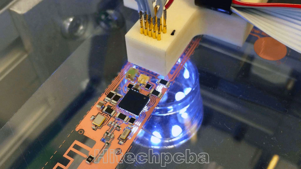
Flexible PCB (Flexible Printed Circuit, FPC) is very popular with excellent characteristics such as low weight and thin thickness, etc. It is also can be folded freely. Flexible PCB mainly relies on manual visual inspection with high cost and low efficiency. With the rapid development of the electronics industry, the design of printed circuit board has become more and more high -precision and high- density, traditional manual testing methods can no longer meet production needs. FPC defect automation testing has become an inevitable trend of industrial development.
Flexible printed circuit (FPC) is a technology developed by the
Flexible PCB includes single sided FPC, double sided FPC and multilayer FPC, etc. Single FPC has chemically etched conductive pattern layer, the conductive pattern layer on the surface of the flexible insulating substrate is calendered copper foil. The insulating substrate may be polyimide, polyethylene terephthalate, arylamide fiber ester and polyvinyl chloride. The double sided FPC on both sides of the insulating base has a conductive graphics made of etching, which increases the wiring density of the unit area. Metal hole connects the graphic connection on both sides of the insulation material to form a conductive pathway to meet the flexible design and function. The covering film can protect the single, double -sided wire and indicate the position of the component placed. According to demand, metal holes and coverage layers are optional. This type of Flexible PCB has fewer applications. Multi -layer flexible PCB is to press the single-sided or double-sided flexible circuit layer of 3 or more layers together. The metal hole is formed by drilling and electroplating, and conductive channels are formed among different layers. In this way, there is no need to use a complex welding process. Multi-layer circuits have huge functional differences in higher reliability, better thermal conductivity and more convenient assembly performance.
At present, the production process of flexible PCB mainly includes looping, Sizing conductor, etching, routing of the conductors, ground planes, sizing of the holes, filleting, button plating, adhesive-backed films, screen-print liquid overcoats, photo imaginable liquid, film polymers and other processes. See the figure for the specific production process.


0086-755-29970700
sales@hitechpcb.com; sales@hitechcircuits.com
3F, B5 Dong, Zhimeihuizhi, FuYong, Bao’an Dist. Shenzhen, GuangDong, China 518103


