 Chinese
 English
 Russian
 Spanish
 Portuguese
High Density PCB board (HDI PCB) Manufacturing
 Add To Cart
Contact Us
Add To Cart
Contact Us
Description
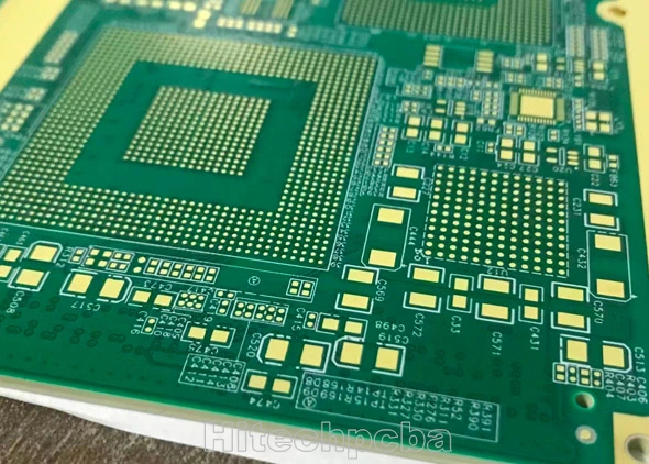
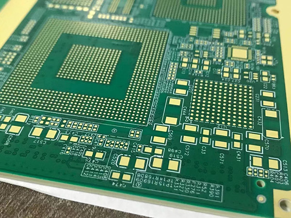
High Density PCB board (HDI PCB) Manufacturer & Assembly – One-stop services
What’s HDI PCB?
High-density interconnect (HDI) PCBs are characterized by finer lines, closer spaces, and more dense wiring, which allow for a faster connection while reducing the size and bulk of a project. These boards also feature blind and buried vias, laser ablated microvias, sequential lamination, and via in-pads.
As a result, a HDI board can house the functionality of the previous boards used. HitechPCB is an HDI PCB manufacturer and provider in Shenzhen,

HDI PCB Manufacturing Process
The overall process for manufacturing HDI PCB is essentially the same as for fabricating other PCB board, with notable differences for PCB stack-up and hole drilling. Since HDI boards generally require smaller drill holes for vias, laser drilling is usually required. Although laser drills can produce smaller and more precise holes, they are limited by depth. Therefore, a limited number of layers can be drilled through at a time. For HDI boards, which are invariably multilayer and may contain buried and blind vias, multiple drilling processes may be required. This necessitates successive layer boding to achieve the desired stack-up or sequential lamination cycles. Not surprisingly, this can significantly increase PCB manufacturing time and cost.
HDI PCB fabrication is an advanced technology and therefore requires expertise along with specialized equipment like laser drills, laser direct imaging (LDI) capability, and special clean room environments. In order to efficiently manufacture high-quality and reliable HDI PCB products, you must understand the HDI board manufacturing process and coordinate with your HDI PCB supplier to implement good DFM (Design for Manufacturability) for HDI layout design.
HDI Printed Circuit Board Development
HDI printed circuit boards were developed from a need to provide an increased level of computational power and performance in a smaller envelope. This need was driven largely by industries such as telecommunications, where the push to provide smaller and more powerful mobile phones necessitated finding a way to package more electronic circuitry in a smaller, denser package. However, other key drivers in the development of HDI PCBs were the trends in Integrated Circuit (IC) technology that acted as a forcing function to reconsider how printed circuit board layouts and interconnects were designed. Some of these key IC technology trends include:
The shrinking size of gates
Reduction in die size
Reduction in operating voltage levels to control power dissipation
Higher levels of gate integration (i.e. more transistors per unit area on a die)
Faster signal rise times (higher operating frequencies and clock rates)
The trend in the packaging of ICs has also shifted away from the use of low-count peripheral lead frame packages towards surface mount technology, allowing the placement of interconnecting pins underneath the entire surface area of the IC. One such technology is the Ball Grid Array (BGA), which places the interconnecting pins in a grid pattern on the underside of the IC. As more and more pins are added to the IC packages, the corresponding density of pins increases, and the dimensional spacing for the circuit board traces or pads decreases (known as the pitch). While this helps with the objective of shrinking the package size for the electronics, it also adds challenges and necessitates changes to the manufacturing process for HDI PCBs.
BGAs do have other advantages, such as lower thermal resistance between the device and the PCB. This fact helps with maintaining acceptable device operating temperatures for chips that are increasingly complex in terms of transistor density. Another advantage of grid array packaging is that the interconnecting leads are shorter. Shorter leads reduce inductance in the leads, which mitigates signal distortion in high-speed circuits, improving overall performance.
Advantages of HDI Printed Circuit Boards
HDI technology provides several advantages and benefits for designers and engineers.
Compact design – HDI boards have high wiring capacity and can reduce both the size and the number of layers needed to produce a design versus using traditional PCBs.
The use of micro vias and via in pad technology allows for components to be placed closer together and more components to be mounted on one side of the board, resulting in faster signal transmission and improved signal integrity due to shorter signal paths.
Laser drilling produces smaller holes and improves the board’s heat resistance.
The ability to reduce the number of layers needed in the PCB design can result in lower costs.
Low pitch devices such as BGAs whose pitch may be 1 mm or less can be supported.
The lower aspect ratio in HDI vias improved the plating of vias and overall board reliability.
Applications for HDI Printed Circuit Boards
HDI printed circuit boards have enabled more electronics to be packed into a smaller envelope, helping to reduce the size of products in a number of markets. Some example of HDI PCB applications include:
Healthcare and medical – implanted devices such as cardiac pacemakers and external devices such as hearing aids.
Automotive industry – smaller, lighter electronics save space and reduces vehicle weight.
Consumer devices – cellular phones, tablets, laptop computers, and touch screen products have all been reduced in size and weight with increased performance due to HDI technology.
Aerospace – electronic designs for missile systems, aircraft, and defense applications utilize HDI printed circuit boards that provide reliable operation in extreme environmental conditions.

0086-755-29970700
sales@hitechpcb.com; sales@hitechcircuits.com
2F, Building C, Suojia Technology Park, Hangcheng, Bao’an, Shenzhen, Guangdong, China 518126


