Epoxy Filled Vias
Via in Pad PCB Manufacturer & Assembly – One-stop service
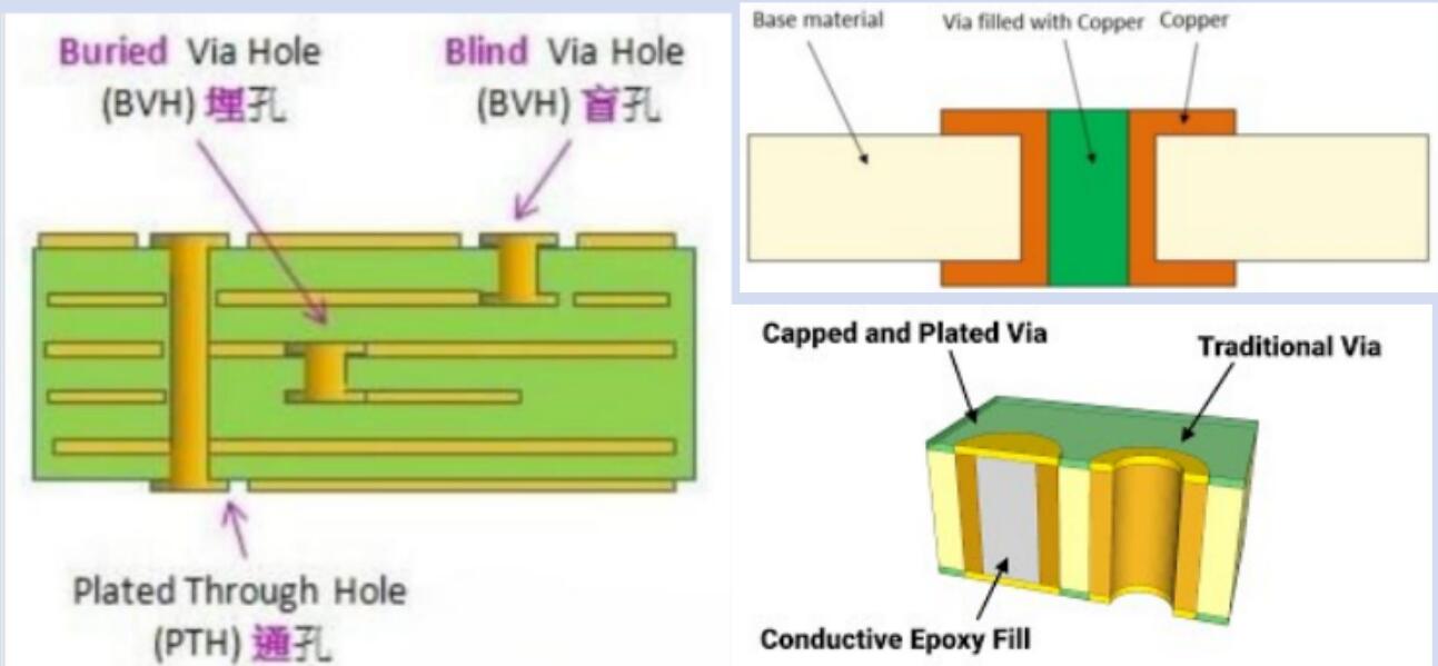
With the increasing trend of miniaturization of electronic products and applications of finer pitch devices, vias become extremely popular since they are an effective solution responsible for electrical connection between traces from different layers in a printed circuit board. Vias can be classified into three main types: Through-hole Vias, Blind Vias and Buried Vias, each of which implements different attributes and functions contributing to the overall optimal performance of PCBs or even electronic products.

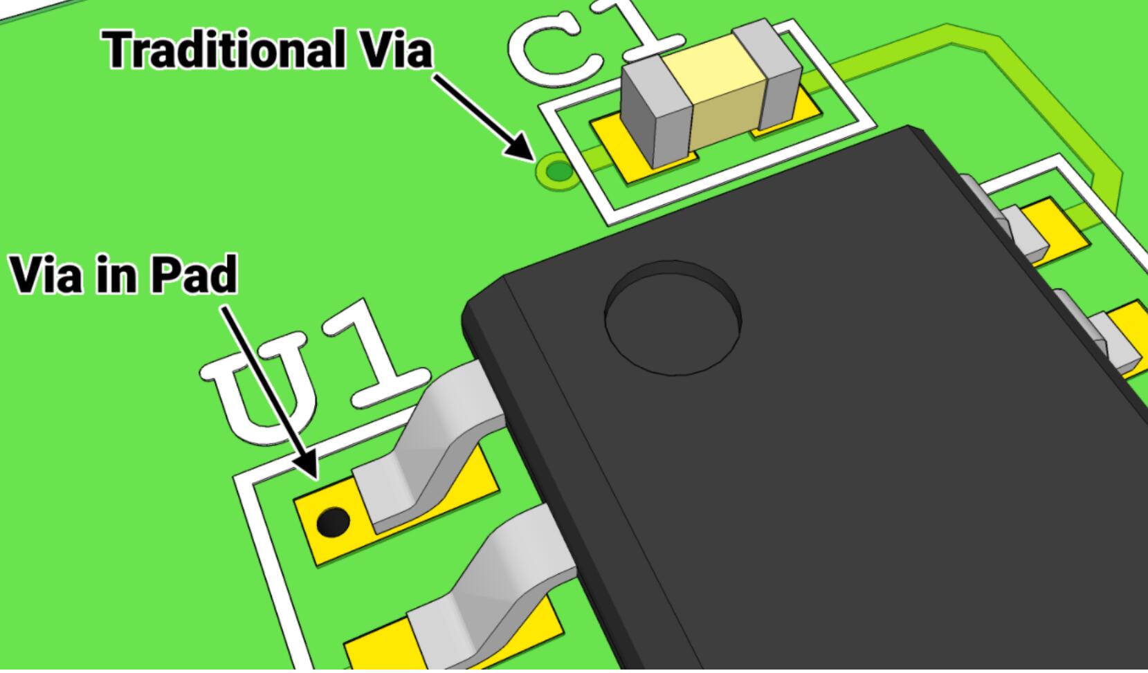
Via-in-pad (VIP) technology basically refers to the technology by which via is placed directly beneath component contact pad, especially BGA pad with finer pitch array packages. In other words, VIP technology leads to vias plated or hidden under BGA pad, requiring that PCB manufacturer should plug via with resin prior to carrying out copper plating on the via to make it invisible.
Hitechpcb offers a variety of printed circuit board manufacturing solutions for Plug Via Process requirements. Whether you require vias flooded with mask, selective plugging in BGA areas, conductive and non-conductive epoxy fill, or fully plugged and via in pad, we have you covered.
In HDI PCB design, via refers to a pad with a plated hole that connects copper tracks from one layer of the board to other layer(s). High-density PCB, multi-layer PCBs may have blind vias, which are visible only on one surface, or buried vias, which are visible on neither, normally referred to as micro vias. The advent and extensive use of finer pitch devices and requirements for smaller size PCBs creates new challenges. An exciting solution to these challenges uses a recent, but common PCB manufacturing technology with self descriptive name, “via in pad”.
Filled via in pad is a way to achieve intermediate density with an intermediate cost compared to using blind/buried vias. Some of the key advantages associated with using the via in pad technology are:
• Fit for fine pitch BGAs
• Leading to higher density of PCBs and promoting space saving
• Performing better in thermal management, beneficial for heat dissipation
• Defeating constraints of high-speed designs such as low inductance
• Sharing a flat surface with component attachment
• Making PCB footprints smaller and routing further and better
Owing to those advantages of VIP technology, via in pad PCB technology is widely applied in small-scale PCBs, especially those that require limited space for BGAs and focus on heat transferring and high-speed PCB designs. Therefore, although blind/buried vias are beneficial for density improvement and PCB real estate saving, as far as heat management and high-speed design elements are concerned, via in pad is still the best choice for you. With cost considered, different projects lead to different cost. So if vias are involved in your project and you fail to pick up which type, contact us through email sales@hitechpcb.com and our staff will provide you an optimal solution.

Via in pad PCB:
In PCB design, via refers to a pad with a plated hole that connects copper tracks from one layer of the board to other layer(s). High-density multi-layer PCBs may have blind vias, which are visible only on one surface, or buried vias, which are visible on neither, normally referred to as micro vias. The advent and extensive use of finer pitch devices and requirements for smaller size PCBs creates new challenges. An exciting solution to these challenges uses a recent, but common PCB manufacturing technology with self descriptive name, “via in pad”.
Via in pad helps to reduce inductance, increase density and employ finer pitch array packages. The via in pad approach places a via directly under the device’s contact pads. This allows higher component density and improved routing. Consequently, via in pad provides the designer significant PCB space savings. For example, traditional fan-out places four components, whereas with via in pad, six components can be placed within the same board outline.
Filled via in pad is a way to achieve intermediate density with an intermediate cost compared to using blind/buried vias. Some of the key advantages associated with using the via in pad technology are:
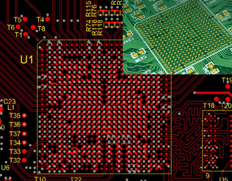
Fan out fine pitch (less than .75mm) BGA
Meets closely packed placement requirements
Better thermal management
Overcomes high speed design issues and constraints i.e. low inductance
No via plugging is required at component locations
Provides a flat, coplanar surface for component attachment
The benefits of via-in-pad designs are well documented. From reduction of inductance to increased density, via-in-pad has become an essential tool for designers when navigating the routing challenges of fine pitch array packages that have become mainstays in today’s BOMs but there are trade-offs that must be considered.
The basic concept is elegant. The via-in-pad design methodology allows the designer to place the via right beneath the component contact pad. Hence the reduction of inductance plus the added benefit of improved routing density which can lead to higher density per layer. The net result is more routing in less space and a smaller PCBs footprint. It is another miniaturization tool that can drive cost down.
However, there are trade-offs when implementing via-in-pad technology. The process may increase the PCB cost. The reason is that the via-in-pad technique requires both additional process steps and extra materials. Added costs are found in both the extra materials used, including epoxy or metal based via fill materials and copper cap plating processes, as well as added process steps like vacuum via fill, curing, planarization and secondary plating operations. There is also the general challenge that results from producing a higher density PCB.

What is via in pad PCB technology?
1. Plug the via by solder mask.
This solution is suitable for big solder SMD pads,
No cost addition.
The standard LPI solder mask process cannot tent of fill vias without the risk of exposed copper inside the hole barrel.
Typically, a secondary screen print operation is used that deposits, UV or thermally curable epoxy soldermask into the holes to plug them. This is called via plugging. Via plugging is used to plug via holes with a solder mask material to prevent air leakage during in circuit test, or to prevent short in from components that are close to the board surface.
2. Plug the via by resin and plated it flat by copper.
It is suitable for small BGA via in pad.
This process fill the via hole with a conductive or nonconductive material and then the via surface is plated over,to provide a smooth flat solderable surface.
There are used for Via-in-pad designs where component may be mounted over the via, or a solder joint will extend over the via connection.
3. Microvias and via in pad plated over.
According to IPC, a microvia is a hole with a diameter of < 0.15mm.
It can be a through viahole (with all respect to a aspect ratio), but we normally see them as blind vias between 2 layers. Mostly drilled by laser, but some pcb manufacturers are also drilling mircorvias with a mechanical drill bit. It is slower, but the holes have a clean and nice cut. The microvia copper fill process is an electrochemical deposition process applied in the manufacturing of multilayer process, also called capped vias.
The process is complex, copper filling of microvias is available from most PCB manufacturers, that are capable of producing HDI PCB Boards.
Via in pad Computer PCB boards:
Prior to the invention of the microprocessor PCB, a computer consisted of multilayer printed circuit boards in a card-cage case with components connected by a backplane, a set of interconnected sockets. In very old designs the wires were discrete connections between card connector pins, but printed circuit boards soon became the standard practice PCB. The Central Processing Unit, memory and peripherals were housed on individual printed circuit boards which were plugged into the backplate.
During the late 1980s and 1990s, it became economical to move an increasing number of peripheral functions onto the motherboard. In the late 1980s, personal computer motherboards began to include single ICs (also called Super I/O chips) PCB capable of supporting a set of low-speed peripherals: keyboard, mouse, floppy disk drive PCB, serial ports, and parallel ports. By the late-1990s, many personal PCB computer motherboards supported a full range of audio, video, storage, and networking functions without the need for any expansion cards at all; higher-end systems for 3D gaming and computer graphics typically retained only the graphics card as a separate component PCB.
The most PCB popular computers such as the Apple II and IBM PC had published schematic diagrams and other documentation which permitted rapid PCB reverse-engineering and third-party replacement motherboards. Usually intended for building new computers compatible with the exemplars PCB, many motherboards offered additional performance or other features and were used to upgrade the manufacturer's original equipment.

 Chinese
 English
 Russian
 Spanish
 Portuguese


