HDI Micro vias PCB
What Blind & Buried Via HDI PCB?
HDI PCB is a circuit board which has a larger wiring density per unit area compared to a conventional board. The HDI in HDI PCB means High Density Interconnection.
What is a Via?
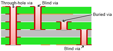
Vias are the copper-plated holes in the PCB that allows the layers to connect. The standard via is called a through-hole via, but there are several disadvantages to using through-hole vias in Surface Mount Technology (SMT). For this reason, we often use a blind via or buried via instead. A blind or buried via can be processed in a wide range of different measures, including plugged copper mask via, a plugged solder mask via, plated via or staggered via.

What is Blind Via?
In a blind via, the via connects the external layer to one or more inner layers of the PCB and is responsible for the interconnection between that top layer and the inner layers.
What is Buried Via?
In a buried via, only the inner layers of the board are connected by the via. It is "buried" inside the board and not visible from the outside.
Blind and buried vias are particularly advantageous in HDI board because they optimize the density of the boards without increasing board size or the number of board layers you require.
What is Stacked Via and Microvia?

A stacked via is a way to further improve size and density considerations when manufacturing PCBs — factors that are extremely important with today's miniaturization and high-signal transmission speed requirements in many applications.
If you have blind vias with an aspect ratio greater than 1:1, or your drilling needs cover multiple layers, a stacked via can be the best way to get a reliable internal connection.
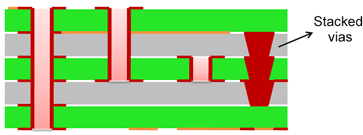
Stacked vias are laminated blind or buried vias, multiple vias inside a circuit board built together around the same center. Staggered vias are laminated vias that are not around the same center. The advantages of stacked vias include not only saving space and increasing density, but greater flexibility concerning the inner connections, better routing capacity and less parasitic capacitance. The downside of stacked vias is that they come with a higher cost than standard through-hole vias or blind/buried vias.
A microvia is merely a very small via. As you can imagine, microvias are very desirable to PCB designers — the smaller the diameter, the more routing space you have on the board and the lower the parasitic capacitance, which is essential for high-speed circuits. However, very small vias also require more drilling time and more off-center via moves. Hitechpcb defines microvias as vias with diameters of less than 0.1mm.
High-Density Interconnection PCB (HDI PCB) is a type of circuit board that features more properties than what we have had on the other Printed Circuit Boards (PCBs).
It has a higher quantity of interconnections and at the same time, occupy a smaller space. Components are placed closer to each other but functionality is still of top quality. A PCB with 120 to 160 pins per square inch is already an HDI PCB. The circuitry is executed with the use of microvias, buried vias and blind vias and imbedded through laser drilling.
Computers that you use are no longer bulky. They have become more fashionable, sleek and chic. HDI PCBs have enabled them to be smaller, just like human models on the fashion ramp who need to be thin so that they can fit into the clothes that they market. These devices no longer have the utilitarian look which leaves nothing to the imagination.
You can also watch Netflix movies on your super thin smartphones, which at times, have even more powerful circuit boards than your PCs and laptops, or also plug in your wireless headphone which also has its own well designed HDI PCB and enjoy the lifelike acoustics.
In addition to the better wiring that it provides, the HDI PCB also provides more number of interconnections and more organized assembly of the electrical components. The outcome of the structuring is that the size and weight of the electrical components will be reduced. That is partly because of the closer placement of the components and mainly because of the significant reduction of the board space.
By and large, the HDI PCB does a great job of enhancing the electrical performance of the circuit board without compromising on the functionalities.

Blind via and Buried Via
When PCB space is limited, or you’re working with tight plated through hole constraints, Blind and Buried Vias may be the answer.
Blind & Buried Via technology has played a pivotal role in squeezing more capability into a smaller space. By shortening vias to only pass through necessary layers, more surface area become available for components.
Blind and buried vias are used to connect between layers of a PCB where space is at a premium. A Blind Via connects an outer layer to one or more inner layers but does not go through the entire board. A Buried Via connects two or more inner layers but does not go through to an outer layer.
Key benefits include:
1. Ability to meet the density constraints of lines and pads on a typical design without increasing the layer count or board size
2. PCB aspect ratio reduction
3. Blind Via is a copper plated hole that connects only one outer layer to one or more inner layers. A blind via never goes all the way through a circuit board. In terms of design, blind vias are defined in a separate drill file.
HDI PCB: Types
HDI PCB comes in different types. Although they are different, with respect to designs, they have the same function. The type you decide to choose depends on the application you are using. Let’s quickly consider the types.
Flex HDI PCB
Flex HDI PCB is composed of flexible plastic. This material permits the board to form different shapes. This offers lots of benefits when compared with rigid boards.
The board’s flexibility also allows you to move or bend easily during the process of application without bringing damage to the circuits that are present on the board. One disadvantage with this board type is that designing and manufacturing it costs a lot. However, they come with numerous benefits.
The heavy wiring found in advanced equipment like satellites can be replaced with these PCBs. They are lighter and make use of little space, making them great for such use. Another benefit is that it features different designs like multilayer, single-sided, or double-sided designs.
Rigid HDI PCB
Asides the number of layers and sides that this HDI PCB has, it also comes in different rigidities. They are made up of a solid and rigid substrate material such as fiberglass. This kind of material prevents the bending of the HDI board. The application of this HDI PCB can be found on towers of most desktops.
Rigid-Flex HDI PCB
This is made up of a rigid circuit board, which attaches to a flexible board. The design’s complexity depends on whatever application you are using.
Multilayer HDI PCB
These boards have substrate boards of multiple layers with an insulating material that separates these layers. Just like HDI PCBs with double sides, either vias or through holes can be used in connecting the board’s electric circuits. Multilayer HDI PCBs are very beneficial because they use less space. Standard applications using this HDI board type include medical machinery, servers, handheld devices, and computers.

 Chinese
 English
 Russian
 Spanish
 Portuguese


