 Chinese
 English
 Russian
 Spanish
 Portuguese
Industry News
Electronics Assembly Services from China - Hitechpcba
Electronics Assembly Services from China – Hitechpcba
In this guidance, you will get some information about the below:
What is electronic assembly service?
What are the main contents of electronic assembly services?
How to do SMT well?
What is the conformal coating?
Something special about the stencil
Now that full turnkey PCB assembly allows PCB designers to make better use of their time to focus more on PCB design, it works perfectly on companies striving for frequent upgrading and refreshing of products. They need to dig into deeper market by providing multiple creative electronic products and they strongly call for a steady and smooth electronic assembly process. Turnkey printed circuit board assembly is also an ideal electronic assembly solution for small businesses or startup companies that want to bring smaller quantities of assembled PCBs to market without having to invest in or carry an extensive inventory. It also offers a more cost-effective, efficient means of assembling and testing PCB prototypes for new products. In addition, quick-turn PCB assembly service makes sense for any company that needs to receive their circuit boards with the shortest possible lead time. These are something about the electronics assembly service.
Hitech Circuits provides electronics assembly manufacturing services for over 15 years. As a global leader in high-mix low-volume manufacturing, we see first-hand the evolution the EMS industry and electronics assembly services are experiencing and the critical role we play in the electronics value chain. In this new guide, you’ll learn something useful about the electronics assembly services and key points which need to be taken much care of. It has many advantages and applications within a variety of technology fields. Meticulous planning and attention to detail is required in the placement and spacing of components, hole sizes and location, component lead spacing, the selection and choice of the components themselves, and other considerations with regard to PCB design, etc.
It is also important to consider something when outsourcing the manufacturing of your product. Hitech provides all kinds of PCBA manufacturing in industrial, Robotic, AI automotive medical electronic control area. In order to estimate the project cost, please send your PCB files and BOM list to sales@hitechpcb.com, You will get quote very soon

Electronic assembly service process includes the below:
1. The basic requirement for assembly preparation is to ensure sufficient quantity and matching of components of PCBs and components. And the quality must be qualified.
2. The processing and fabrication of the connection cable are mainly based on the design documents, processing all kinds of connecting cable used in the whole assembly process to meet the production process requirements.
3. PCBA assembly is mainly to install capacitors, resistors, transistors, integrated circuits and other electronic components on the PCB board according to the requirements of the design documents, which is the basis for manufacturing turnkey electronic products.
4. Unit assembly is based on PCB assembly, combining PCB components through the interface and connecting cable into units or modules with specific functions.
5. The turnkey assembly is based on the unit assembly, and the various unit components that make up the electronic product are installed in a unified cabinet, cabinet or other carriers, and finally become a complete electronic product.
6. Turnkey assembly debugging and testing. Commissioning and testing are required after turnkey assembly. The turnkey assembly debugging mainly includes two parts of adjustment and test.
7. Adjustment is a working process to adjust the adjustable part of the electronics products to enable it can complete the normal working. This test is a comprehensive test of the function and performance of the assembled machine. The test can achieve the predetermined technical indicators and whether the predetermined function can be achieved.
8. The final inspection is the finished part of the assembly of the entire electronic products. It is mainly to carry out a comprehensive inspection of all aspects of the adjusted turnkey pcb assembly to detect whether the product is a qualified product.
What is Electronics Assembly Services, also called Electronic Manufacturing Services (EMS)?
Electronic Manufacturing Services refers to a range of electronic product design, development, and manufacturing services offered by EMS companies. Depending on the type of EMS company, they either offer only product development and design services, or they offer both product design and manufacturing services. As technology continues to evolve, so does the world of electronics, and with that in mind, EMS are experiencing rapid growth within the industry. An EMS company offers more than just a contract manufacturing service. They offer total solutions, including development, engineering, industrial design, and production management. Various factors are attributed to the growth of the EMS industry. Some of these factors are:
1. The need for more cost-competitive products
2. Development and deployment of smaller and less complex products
3. Increasing globalization in the electronics industry and
4. New commercialization strategies in the consumer electronics sector.
The Services Offered by EMS Companies
As already stipulated, diverse EMS companies exist across the world. Each electronic manufacturing service company offers services that may vary from competitors. However, every EMS Company should offer the following electronic manufacturing services.
That is Printed circuit board assembly. The assembly of PCBs is one key electronic service that almost every EMS Company offers. It can entail surface mount or through-hole tech methods of soldering the PCB components on the circuit board. Additionally, the components range from integrated circuits, transistors to resistors. But since most of these components are tiny, having a machine to pick and place besides aligning them becomes key, something you realize with EMS companies.
Turnkey Electronic assembly manufacturing
1.The fittings (include components & assembly unit) that have not passed the inspection shall not be installed, and the assembled parts that have passed the inspection shall be kept clean.
2. Read the process documents and design documents carefully and strictly abide by the technical procedures. The completed turnkey assembly shall meet the requirements of drawings and technical documents.
3. Strictly follow the general sequence of assembly, prevent the order of the front and back from being reversed, and pay attention to the process connection between the front and the back.
4. Do not damage the components during the assembly process, to avoid damage to the coating on the machine case and components, so as not to damage the insulation performance.
5.Requires proficiency in operational skills, quality assurance, and strict implementation of inspection, mutual inspection, and full-time inspection.
Brief Electronic Assembly Process
A typical electronic assembly process includes: solder paste printing, mounting, reflow soldering, wave soldering, testing, etc.
These processes are described below:
1. Applying the solder paste
Solder paste printing is the first process in the SMT process, which uses a printing machine to leak solder paste from the stencil opening onto the PCB pad. According to statistics, 60%~70% of soldering defect are caused by poor solder paste printing. To achieve high-quality solder paste printing, in addition to considering the selection of solder paste and solder paste printing parameters, specific requirements are also put forward for PCB board design and processing.
2. SMT
SMT technology is a key process in the assembly and production of SMT products. The installation of SMC/SMD (surface mount components) is generally carried out automatically using a mounting machine. The SMT mounting machine is the core equipment in the SMT product assembly production line and also a key equipment of SMT, which determines the degree of automation in SMT product assembly.
The main actions of SMT include substrate positioning, component picking, component positioning, component SMT, etc. To achieve high-quality SMT quality and efficiency, specific requirements are also put forward for PCB board design.
3. Reflow soldering
Reflow soldering refers to the process of group welding of PCBA with mounted components through reflow soldering furnace. reflow soldering is an important process of SMT process.
4. Soldering assembly
The welding assembly method is mainly applied to the connection between components and printed boards, the connection between wires and printed boards, and the connection between printed boards and printed boards. Its advantages are: good electrical performance, high mechanical strength, compact structure, but its disadvantage is poor disassembly.
5. Pressing assembly
There are two types of pressing: cold pressing and hot pressing. Currently, cold crimping is widely used. pressing is the use of high extrusion force and metal displacement to connect the connector pins or terminals to the wire. The tool used for pressing is a pressing pliers. Place the wire end into the contact foot or end solder joint and press firmly to obtain a reliable connection. The contact pins and solder pads are specialized devices used to connect wires, with various specifications available for selection.
SMT Processing Technology
With the development of technology, many electronic products are moving towards miniaturization and refinement, which has resulted in many SMD components becoming smaller and smaller in size. Not only are the requirements for the processing environment constantly increasing, but higher requirements are also put forward for SMT processing technology. Nowadays, in order to do a good job in SMT chip processing, factories need to achieve at least the following three points:
1、 In the SMT processing process, everyone knows that solder paste is required. For newly purchased tin products, if not immediately used, they must be stored in an environment of 5-10 degrees Celsius. In order not to affect the use of solder paste, it should not be placed in a minus zero environment.
2、 During the SMT mounting process, it is necessary to regularly inspect the SMT mounting machine equipment. If the equipment is old or some components are damaged, it is necessary to repair or replace the equipment with a new one to ensure that the patches are not bent. Only in this way can production costs be reduced and production efficiency be improved.
3、 In the process of SMT processing, in order to ensure the quality of PCB board welding, we must always pay attention to whether the setting of reflow soldering process parameters is very managed. If there is an issue with the parameter settings, the quality of PCB board welding cannot be guaranteed. So generally speaking, the furnace temperature must be tested twice a day, at least once. Continuously improving the temperature curve and setting the temperature curve of welding products can ensure the quality of processed products.
Nowadays, business in various industries is not easy to do. To survive and develop in the SMT chip processing industry, factories need to do their best and ensure the quality of production, in order to continuously attract customers.
Here is a guide to introduce an important step in the assembly of PCBA: applying the conformal coating.
PCBA conformal coating
PCBA conformal coating is a protective oil, waterproof adhesive, and insulation paint used to prevent moisture, poison, and dust. Therefore, it is called three proof paint. It is mainly used at the rear end of assembly, after SMT chip processing and testing, to perform conformal coating treatment on the surface of the product. There are various processes such as immersion, brushing, spraying, and selective coating. This is what we often refer to as the conformal coating process for printed circuit boards.
Now, let's talk about what to pay attention to when applying the conformal coating:
1. The surface of the product should be cleaned of dust, moisture, and rosin, and the cleaning and baking of the board should be maintained to ensure that the three proofing paint is well adhered to the surface of the circuit board.
2. The brushing area should be evenly distributed to ensure full coverage of components and solder pads. Baking conditions: 65 ℃, 15-35 minutes, take out in the oven and apply while hot for better results.
3. When brushing, the PCBA board should be placed on a flat tabletop, and there should be no dripping or exposed parts after brushing. A thickness of 0.1-0.3mm is the most suitable.
4. After coating, place it on a shelf to cure it (heating can also accelerate the curing of the coating).
5. When applying the conformal coating, it should be noted that all high-power heat dissipation surfaces or radiator components, power resistors, power diodes, cement resistors, etc. cannot be coated with the conformal coating. When applying, cover and protect them, and screw holes on the board cannot be coated with the conformal coating.
6. If you want a thicker coating, you can apply two thinner layers and overlay them (the second layer needs to be applied after the first layer has cured).
7. The work of three proofing paint should be carried out in a separate enclosed room with good ventilation facilities. Wear protective gear such as masks and gloves during work to protect the body from harm.
Something special about the stencil
1. For solder paste printing on miniaturized pads, the smaller the pad and the stainless-steel stencil opening, the harder it is for the solder paste to detach from the stainless-steel stencil hole wall. To solve the solder paste printing of miniaturized solder pads, there are several solutions for reference:
The most direct solution is to reduce the thickness of the stainless-steel stencil and increase the ratio of the opening area. As shown in the figure below, after using a thin stainless-steel stencil, the soldering pad of small components has good soldering performance. If the substrate produced does not have large-sized components, then this is the simplest and most effective solution. However, if there are large components on the substrate, the large components will be poorly soldered due to low tin content. So if it is a high hybrid substrate with large components, we need other solutions listed below.
2. Utilize new stainless-steel stencil technology to reduce the requirement for stainless-steel stencil opening ratio.
1) FG (Fine Grain) stainless-steel stencil
FG steel sheets contain a type of niobium element, which can refine grain size, reduce overheating sensitivity and temper brittleness of the steel, and improve strength. The hole wall of FG steel sheet cut by laser is cleaner and smoother than that of ordinary 304 steel sheet, which is more conducive to demolding. The opening area ratio of stainless-steel stencil made of FG steel sheets can be less than 0.65. Compared to 304 stainless-steel stencils with the same opening ratio, FG stainless-steel stencil can be made slightly thicker than 304 stainless-steel stencils, thereby reducing the risk of less tin in large components.
2) Electroformed stainless-steel stencil
The manufacturing principle of electroformed stainless-steel stencil: By printing photoresist material on a conductive metal substrate, and then making a template for electroforming through shielding mold and ultraviolet exposure, the thin template is then electroformed in the electroforming solution. In fact, electroforming is similar to electroplating, except that the nickel sheet after electroforming can be peeled off from the bottom plate to form a stainless-steel stencil.

The electroformed stainless-steel stencil has the following characteristics: there is no stress inside the steel sheet, the hole wall is very smooth, and the stainless-steel stencil can be of any thickness (within 0.2mm, controlled by the electroforming time), but the disadvantage is that the cost is relatively high. The following figure is a comparison of the hole wall diagrams of laser stainless-steel stencil and electroformed stainless-steel stencil. The smooth hole wall of the electroformed stainless-steel stencil has better demolding effect after printing, allowing the hole ratio to be as low as 0.5.
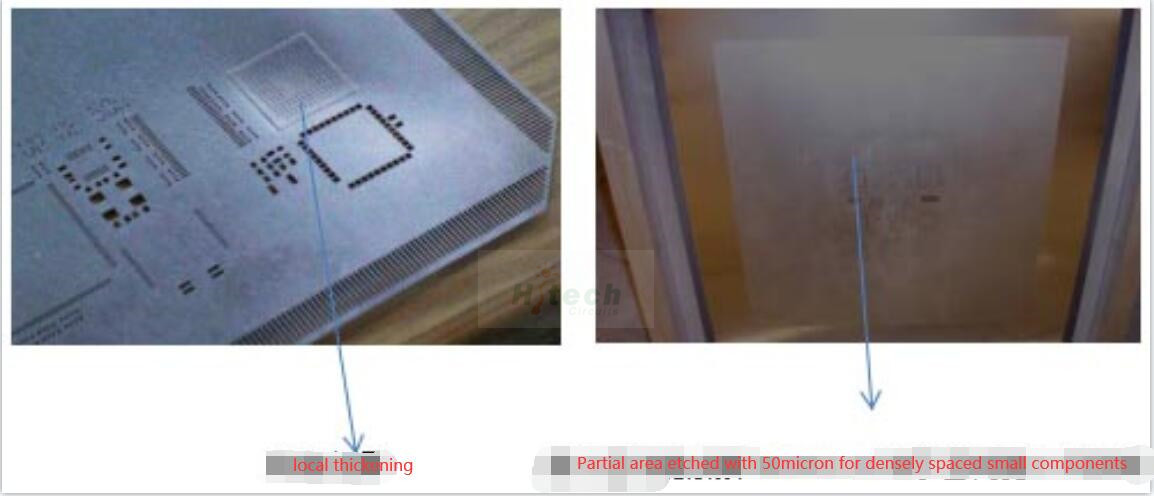
3) Stepped stainless-steel stencil
The stepped stainless-steel stencil can be locally thickened or thinned. The partially thickened part is used to print solder pads with high demand for solder paste, and the thickened part is achieved through electroforming, which is costly. And thinning is achieved through chemical etching, and the thinning part is used to print the solder pads of miniaturized components, making the demolding effect better. For users who are more sensitive to costs, chemical etching is recommended to use, with lower costs.
4) Nano coating. (Nano Ultra Coating)
Coating or plating a layer of nano coating on the surface of the stainless-steel stencil, which repels the hole wall from the solder paste, resulting in better demolding effect and consistent volume stability of solder paste printing. In this way, the quality of printing is relatively guaranteed, while also reducing the number of times the stainless-steel stencil is cleaned and wiped. At present, most of the domestic processes only apply a layer of nano coating, which weakens the effect after a certain number of printing cycles. There are nano coatings directly plated on stainless-steel stencil in foreign countries, which have better effect and durability, and of course, higher costs.
3. Dual solder paste molding process.
1) Printing/Printing
Use two printing machines to print the formed solder paste. The first machine uses ordinary stainless-steel stencil to print small component pads with dense spacing, while the second machine uses 3D stainless-steel stencil or stepped stainless-steel stencil to print large component pads.
This method requires two printing machines, and the cost of stainless-steel stencil is also high. If 3D stainless-steel stencil is used, a comb scraper is also needed, which increases costs and reduces production efficiency.
2) Printing/tin spraying
The first solder paste printing machine printed densely spaced small component solder pads, and the second spray printing machine printed large component solder pads. This method has good solder paste forming effect, but it has high cost and low efficiency (depending on the number of solder pads in large components).

0086-755-29970700
sales@hitechpcb.com; sales@hitechcircuits.com
2F, Building C, Suojia Technology Park, Hangcheng, Bao’an, Shenzhen, Guangdong, China 518126


